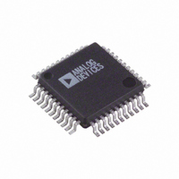
ADV7177KS-REEL Analog Devices Inc, ADV7177KS-REEL Datasheet - Page 29

ADV7177KS-REEL
Manufacturer Part Number
ADV7177KS-REEL
Description
IC DAC VIDEO NTSC 3-CH 44MQFP
Manufacturer
Analog Devices Inc
Type
Video Encoderr
Datasheet
1.ADV7177KSZ-REEL.pdf
(44 pages)
Specifications of ADV7177KS-REEL
Rohs Status
RoHS non-compliant
Applications
Set-Top Boxes, TV
Voltage - Supply, Analog
3 V ~ 3.6 V
Mounting Type
Surface Mount
Package / Case
44-MQFP, 44-PQFP
Adc/dac Resolution
9b
Screening Level
Commercial
Package Type
MQFP
Pin Count
44
Voltage - Supply, Digital
-
Lead Free Status / RoHS Status
Not Compliant
SUBCARRIER
SUBCARRIER
SUBCARRIER
Program as
Figure 34 shows how the frequency is set up by the four
registers.
SUBCARRIER
SUBCARRIER PHASE REGISTER (FP7–FP0)
Address [SR4–SR0] = 06H
This 8-bit-wide register is used to set up the subcarrier phase.
Each bit represents 1.41 degrees.
TIMING REGISTER 0 (TR07–TR00)
Address [SR4–SR0] = 07H
Figure 37 shows the various operations under the control of
Timing Register 0. This register can be read from as well as
written to. This register can be used to adjust the width and
position of the master mode timing signals.
TR0 BIT DESCRIPTION
Master/Slave Control (TR00)
This bit controls whether the ADV7177/ADV7178 are in master
or slave mode. This register can be used to adjust the width and
position of the master timing signals.
Timing Mode Selection (TR02–TR01)
These bits control the timing mode of the ADV7177/ADV7178.
These modes are described in the Timing and Control section.
FREQUENCY
FREQUENCY
FREQUENCY
FREQUENCY
FSC Register 0: 1Fh
FSC Register 2: 7Ch
FSC Register 3: F0h
FSC Register 4: 21h
REG 3
REG 2
REG 1
REG 0
FSC23
FSC15
FSC31
FSC7
Figure 34. Subcarrier Frequency Register
FSC22 FSC21
FSC14 FSC13
FSC30 FSC29
FSC6
REGISTER RESET
TR07
FSC5
TIMING
TR07
FSC20
FSC12
FSC28
FSC4
TR06
PIXEL PORT
FSC19
FSC11
FSC27
FSC3
CONTROL
0
1
TR06
8-BIT
16-BIT
FSC18
FSC10
FSC26
FSC2
TR05
FSC17
FSC25
FSC9
FSC1
TR05
0
0
1
1
TR04
LUMA DELAY
0
1
0
1
FSC16
FSC24
FSC0
FSC8
Figure 37. Timing Register 0
0ns DELAY
74ns DELAY
148ns DELAY
222ns DELAY
TR04
Rev. C | Page 29 of 44
TR03
BLANK INPUT
0
1
CONTROL
TR03
ENABLE
DISABLE
Input Control (TR03)
This bit controls whether the BLANK input is used when the
part is in slave mode.
Luma Delay (TR05–TR04)
These bits control the addition of a luminance delay. Each bit
represents a delay of 74 ns.
Pixel Port Control (TR06)
This bit is used to set the pixel port to accept 8-bit or 16-bit
data. If an 8-bit input is selected, the data is set up on
Pins P7–P0.
Timing Register Reset (TR07)
Toggling TR07 from low to high and low again resets the
internal timing counters. This bit should be toggled after
power-up, reset, or after changing to a new timing mode.
CLOSED CAPTIONING EVEN FIELD
DATA REGISTER 1–0 (CED15–CED0)
Address [SR4–SR0] = 09H–08H
These 8-bit-wide registers are used to set up the closed
captioning extended data bytes on even fields. Figure 35
shows how the high and low bytes are set up in the registers.
CLOSED CAPTIONING ODD FIELD
DATA REGISTER 1–0 (CCD15–CCD0)
Subaddress [SR4–SR0] = 0BH–0AH
These 8-bit-wide registers are used to set up the closed
captioning data bytes on odd fields. Figure 36 shows how
the high and low bytes are set up in the registers.
BYTE 0
BYTE 0
TR02
BYTE 1
BYTE 1
0
0
1
1
TIMING MODE
TR02
SELECTION
TR01
CCD7
CED7
0
1
0
1
CED15
CCD15
Figure 35. Closed Captioning Extended Data Register
MODE 0
MODE 1
MODE 2
MODE 3
CCD6
CED6
Figure 36. Closed Captioning Data Register
TR01
CED14 CED13
CCD14 CCD13
TR00
0
1
CCD5
CED5
MASTER/SLAVE
SLAVE TIMING
MASTER TIMING
CONTROL
TR00
CCD4
CED4
CCD12
CED12
CCD3
CED3
CCD11
CED11
ADV7177/ADV7178
CCD2
CED2
CCD10
CED10
CCD1
CED1
CCD9
CED9
CCD0
CED0
CCD8
CED8


