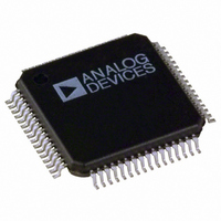
ADV7180BSTZ Analog Devices Inc, ADV7180BSTZ Datasheet - Page 62

ADV7180BSTZ
Manufacturer Part Number
ADV7180BSTZ
Description
IC VIDEO DECODER SDTV 64-LQFP
Manufacturer
Analog Devices Inc
Type
Video Decoderr
Datasheet
1.ADV7180BSTZ.pdf
(116 pages)
Specifications of ADV7180BSTZ
Design Resources
Low Cost Differential Video Receiver Using ADA4851 Amplifier and ADV7180 Video Decoder (CN0060) Low Cost Video Multiplexer for Video Switching Using ADA4853-2 Op Amp with Disable Function (CN0076)
Applications
Digital Cameras, Mobile Phones, Portable Video
Voltage - Supply, Analog
1.71 V ~ 1.89 V
Voltage - Supply, Digital
1.65 V ~ 2 V
Mounting Type
Surface Mount
Package / Case
64-LQFP
Resolution (bits)
10bit
Input Format
Analog
Output Format
Digital
Adc Sample Rate
57.27MSPS
Power Dissipation Pd
15µW
No. Of Input Channels
6
Supply Voltage Range
1.71V To 1.89V
Lead Free Status / RoHS Status
Lead free / RoHS Compliant
For Use With
EVAL-ADV7180LQEBZ - BOARD EVALUATION ADV7180EVAL-ADV7180LFEBZ - BOARD EVAL FOR ADV7180 LFCSP
Lead Free Status / RoHS Status
Lead free / RoHS Compliant, Lead free / RoHS Compliant
Available stocks
Company
Part Number
Manufacturer
Quantity
Price
Company:
Part Number:
ADV7180BSTZ
Manufacturer:
AMIS
Quantity:
6 240
Company:
Part Number:
ADV7180BSTZ
Manufacturer:
Analog Devices Inc
Quantity:
10 000
Part Number:
ADV7180BSTZ
Manufacturer:
ADI/亚德诺
Quantity:
20 000
Company:
Part Number:
ADV7180BSTZ-REEL
Manufacturer:
Analog Devices Inc
Quantity:
10 000
ADV7180
CGMS and WSS
The CGMS and WSS data packets convey the same type of
information for different video standards. WSS is for PAL and
CGMS is for NTSC; therefore, the CGMS and WSS readback
registers are shared. WSS is biphase coded; the VDP performs a
biphase decoding to produce the 14 raw WSS bits in the CGMS/
WSS readback I
CGMS_WSS_CLEAR, CGMS/WSS Clear, Address 0x78[2],
User Sub Map, Write Only, Self-Clearing
Setting CGMS_WSS_CLEAR to 1 reinitializes the CGMS/WSS
readback registers.
Table 81. CGMS Readback Registers
Signal Name
CGMS_WSS_DATA_0[3:0]
CGMS_WSS_DATA_1[7:0]
CGMS_WSS_DATA_2[7:0]
1
These registers are readback registers; default value does not apply.
+100 IRE
+70 IRE
–40 IRE
2
C registers and to set the CGMS_WSS_AVL bit.
0 IRE
11.0µs
11.2µs
SEQUENCE
1
RUN-IN
2.235µs ± 20ns
Register Location
VDP_CGMS_WSS_DATA_0[3:0]
VDP_CGMS_WSS_DATA_1[7:0]
VDP_CGMS_WSS_DATA_2[7:0]
REF
START
CODE
38.4µs
42.5µs
0
0
VDP_CGMS_WSS_DATA_2
Figure 47. CGMS Waveform
VDP_CGMS_WSS_DATA_2
Figure 46. WSS Waveform
1
1
Rev. F | Page 62 of 116
2
2
3
3
4
4
5
5
CGMS_WSS_AVL, CGMS/WSS Available, Address 0x78[2],
User Sub Map, Read Only
When CGMS_WSS_AVL is 0, CGMS/WSS was not detected.
When CGMS_WSS_AVL is 1, CGMS/WSS was detected.
VDP_CGMS_WSS_DATA_0[3:0], Address 0x7D[3:0];
VDP_CGMS_WSS_DATA_1[7:0], Address 0x7E[7:0];
VDP_CGMS_WSS_DATA_2[7:0], Address 0x7F[7:0];
User Sub Map, Read Only
These bits hold the decoded CGMS or WSS data.
Refer to Figure 46 and Figure 47 for the I
CGMS bit mapping.
6
6
7
7
VDP_CGMS_WSS_
DATA_1[5:0]
0
0
49.1µs ± 0.5µs
1
VDP_CGMS_WSS_DATA_1
1
2
2
3
3
4
4
5
125
126
127
5
6
ACTIVE
Address (User Sub Map)
CRC SEQUENCE
VIDEO
7
VDP_CGMS_WSS_
DATA_0[3:0]
0
1
2
C-to-WSS and I
2
3
0x7D
0x7E
0x7F
2
C-to-


