DS26521LN+ Maxim Integrated Products, DS26521LN+ Datasheet - Page 7
DS26521LN+
Manufacturer Part Number
DS26521LN+
Description
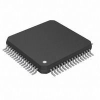
IC TXRX T1/E1/J1 64-LQFP
Manufacturer
Maxim Integrated Products
Type
Line Interface Units (LIUs)r
Datasheet
1.DS26521LN.pdf
(258 pages)
Specifications of DS26521LN+
Number Of Drivers/receivers
1/1
Protocol
T1/E1/J1
Voltage - Supply
3.135 V ~ 3.465 V
Mounting Type
Surface Mount
Package / Case
64-LQFP
Lead Free Status / RoHS Status
Lead free / RoHS Compliant


DS26521 Single T1/E1/J1 Transceiver
LIST OF TABLES
Table 4-1. T1-Related Telecommunications Specifications ...................................................................................... 14
Table 4-2. E1-Related Telecommunications Specifications ...................................................................................... 15
Table 5-1. Time Slot Numbering Schemes................................................................................................................ 16
Table 7-1. Detailed Pin Descriptions ......................................................................................................................... 19
Table 8-1. Reset Functions........................................................................................................................................ 29
Table 8-2. Registers Related to the Elastic Store...................................................................................................... 32
Table 8-3. Elastic Store Delay After Initialization....................................................................................................... 33
Table 8-4. Registers Related to the IBO Multiplexer ................................................................................................. 35
Table 8-5. D4 Framing Mode..................................................................................................................................... 38
Table 8-6. ESF Framing Mode .................................................................................................................................. 39
Table 8-7. SLC-96 Framing ....................................................................................................................................... 39
Table 8-8. E1 FAS/NFAS Framing ............................................................................................................................ 41
Table 8-9. Registers Related to Setting Up the Framer ............................................................................................ 42
Table 8-10. Registers Related to the Transmit Synchronizer.................................................................................... 43
Table 8-11. Registers Related to Signaling ............................................................................................................... 44
Table 8-12. Registers Related to SLC-96.................................................................................................................. 47
Table 8-13. Registers Related to T1 Transmit BOC.................................................................................................. 48
Table 8-14. Registers Related to T1 Receive BOC................................................................................................... 49
Table 8-15. Registers Related to T1 Transmit FDL................................................................................................... 49
Table 8-16. Registers Related to T1 Receive FDL.................................................................................................... 50
Table 8-17. Registers Related to E1 Data Link ......................................................................................................... 50
Table 8-18. Registers Related to Maintenance and Alarms...................................................................................... 52
Table 8-19. T1 Alarm Criteria .................................................................................................................................... 54
Table 8-20. T1 Line Code Violation Counting Options .............................................................................................. 55
Table 8-21. E1 Line Code Violation Counting Options .............................................................................................. 56
Table 8-22. T1 Path Code Violation Counting Arrangements ................................................................................... 56
Table 8-23. T1 Frames Out of Sync Counting Arrangements ................................................................................... 56
Table 8-24. Registers Related to DS0 Monitoring ..................................................................................................... 57
Table 8-25. Registers Related to T1 In-Band Loop Code Generator ........................................................................ 59
Table 8-26. Registers Related to T1 In-Band Loop Code Detection ......................................................................... 60
Table 8-27. Registers Related to Framer Payload Loopbacks.................................................................................. 61
Table 8-28. Registers Related to the HDLC .............................................................................................................. 62
Table 8-29. Recommended Supply Decoupling ........................................................................................................ 69
Table 8-30. Registers Related to Control of DS26521 LIU ....................................................................................... 69
Table 8-31. Telecommunications Specification Compliance for DS26521 Transmitters .......................................... 70
Table 8-32. Transformer Specifications..................................................................................................................... 70
Table 8-33. ANSI T1.231, ITU-T G.775, and ETS 300 233 Loss Criteria Specifications .......................................... 74
Table 8-34. Jitter Attenuator Standards Compliance................................................................................................. 76
Table 8-35. Registers Related to BERT Configure, Control, and Status................................................................... 79
Table 9-1. Register Address Ranges......................................................................................................................... 81
Table 9-2. Global Register List .................................................................................................................................. 82
Table 9-3. Framer Register List ................................................................................................................................. 83
Table 9-4. LIU Register List ....................................................................................................................................... 90
Table 9-5. BERT Register List ................................................................................................................................... 90
Table 9-6. Global Register Bit Map............................................................................................................................ 91
Table 9-7. Framer Register Bit Map .......................................................................................................................... 92
Table 9-8. LIU Register Bit Map .............................................................................................................................. 100
Table 9-9. BERT Register Bit Map .......................................................................................................................... 100
Table 9-10. Global Register Set .............................................................................................................................. 101
Table 9-11. Backplane Reference Clock Select ...................................................................................................... 104
Table 9-12. Master Clock Input Selection................................................................................................................ 104
Table 9-13. Device ID Codes in this Product Family ............................................................................................... 106
Table 9-14. LIU Register Set ................................................................................................................................... 203
Table 9-15. Transmit Load Impedance Selection.................................................................................................... 204
Table 9-16. Transmit Pulse Shape Selection .......................................................................................................... 204
Table 9-17. Receive Level Indication....................................................................................................................... 209
7 of 258
Related parts for DS26521LN+
Image
Part Number
Description
Manufacturer
Datasheet
Request
R

Part Number:
Description:
Ds26521 Single T1/e1/j1 Transceiver
Manufacturer:
Maxim Integrated Products, Inc.
Datasheet:
Part Number:
Description:
power light source LUXEON® Collimator
Manufacturer:
LUMILEDS [Lumileds Lighting Company]
Datasheet:

Part Number:
Description:
MAX7528KCWPMaxim Integrated Products [CMOS Dual 8-Bit Buffered Multiplying DACs]
Manufacturer:
Maxim Integrated Products
Datasheet:
Part Number:
Description:
Single +5V, fully integrated, 1.25Gbps laser diode driver.
Manufacturer:
Maxim Integrated Products
Datasheet:
Part Number:
Description:
Single +5V, fully integrated, 155Mbps laser diode driver.
Manufacturer:
Maxim Integrated Products
Datasheet:
Part Number:
Description:
VRD11/VRD10, K8 Rev F 2/3/4-Phase PWM Controllers with Integrated Dual MOSFET Drivers
Manufacturer:
Maxim Integrated Products
Datasheet:
Part Number:
Description:
Highly Integrated Level 2 SMBus Battery Chargers
Manufacturer:
Maxim Integrated Products
Datasheet:
Part Number:
Description:
Current Monitor and Accumulator with Integrated Sense Resistor; ; Temperature Range: -40°C to +85°C
Manufacturer:
Maxim Integrated Products
Part Number:
Description:
TSSOP 14/A°/RS-485 Transceivers with Integrated 100O/120O Termination Resis
Manufacturer:
Maxim Integrated Products
Part Number:
Description:
TSSOP 14/A°/RS-485 Transceivers with Integrated 100O/120O Termination Resis
Manufacturer:
Maxim Integrated Products
Part Number:
Description:
QFN 16/A°/AC-DC and DC-DC Peak-Current-Mode Converters with Integrated Step
Manufacturer:
Maxim Integrated Products
Part Number:
Description:
TDFN/A/65V, 1A, 600KHZ, SYNCHRONOUS STEP-DOWN REGULATOR WITH INTEGRATED SWI
Manufacturer:
Maxim Integrated Products
Part Number:
Description:
Integrated Temperature Controller f
Manufacturer:
Maxim Integrated Products
Part Number:
Description:
SOT23-6/I°/45MHz to 650MHz, Integrated IF VCOs with Differential Output
Manufacturer:
Maxim Integrated Products