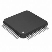
DS26521LN+ Maxim Integrated Products, DS26521LN+ Datasheet - Page 109

DS26521LN+
Manufacturer Part Number
DS26521LN+
Description
IC TXRX T1/E1/J1 64-LQFP
Manufacturer
Maxim Integrated Products
Type
Line Interface Units (LIUs)r
Datasheet
1.DS26521LN.pdf
(258 pages)
Specifications of DS26521LN+
Number Of Drivers/receivers
1/1
Protocol
T1/E1/J1
Voltage - Supply
3.135 V ~ 3.465 V
Mounting Type
Surface Mount
Package / Case
64-LQFP
Lead Free Status / RoHS Status
Lead free / RoHS Compliant
- Current page: 109 of 258
- Download datasheet (2Mb)
9.4
See
9.4.1 Receive Register Definitions
Register Name:
Register Description:
Register Address:
Bit #
Name
Default
Bit 7: Receive CRC-16 Display (RCRCD).
Bit 6: Receive HDLC Reset (RHR). Will reset the receive HDLC controller and flush the receive FIFO. Note that
this bit is a acknowledged reset. The host should set this bit and the DS26521 will clear it once the reset operation
is complete. The DS26521 will complete the HDLC reset within two frames.
Bit 5: Receive HDLC Mapping Select (RHMS).
Bit 4 to 0: Receive HDLC Channel Select 4 to 0 (RHCS[4:0]). These bits determine which DS0 is mapped to the
HDLC controller when enabled with RHMS = 0. RHCS[4:0] = all 0s selects channel 1, RHCS[4:0] = all 1s selects
channel 32 (E1). A change to the receive HDLC channel select is acknowledged only after a receive HDLC reset
(RHR).
Table 9-3
Framer Register Definitions
0 = Do not write received CRC-16 code to FIFO (default)
1 = Write received CRC-16 code to FIFO after last octet of packet
0 = Normal operation
1 = Reset receive HDLC controller and flush the receive FIFO
0 = Receive HDLC assigned to channels
1 = Receive HDLC assigned to FDL (T1 mode), Sa bits (E1 mode)
RCRCD
for the complete framer register list.
7
0
RHC
Receive HDLC Control Register
010h
RHR
6
0
RHMS
5
0
RHCS4
109 of 258
4
0
RHCS3
3
0
DS26521 Single T1/E1/J1 Transceiver
RHCS2
2
0
RHCS1
1
0
RHCS0
0
0
Related parts for DS26521LN+
Image
Part Number
Description
Manufacturer
Datasheet
Request
R

Part Number:
Description:
Ds26521 Single T1/e1/j1 Transceiver
Manufacturer:
Maxim Integrated Products, Inc.
Datasheet:

Part Number:
Description:
power light source LUXEON® Collimator
Manufacturer:
LUMILEDS [Lumileds Lighting Company]
Datasheet:

Part Number:
Description:
MAX7528KCWPMaxim Integrated Products [CMOS Dual 8-Bit Buffered Multiplying DACs]
Manufacturer:
Maxim Integrated Products
Datasheet:

Part Number:
Description:
Single +5V, fully integrated, 1.25Gbps laser diode driver.
Manufacturer:
Maxim Integrated Products
Datasheet:

Part Number:
Description:
Single +5V, fully integrated, 155Mbps laser diode driver.
Manufacturer:
Maxim Integrated Products
Datasheet:

Part Number:
Description:
VRD11/VRD10, K8 Rev F 2/3/4-Phase PWM Controllers with Integrated Dual MOSFET Drivers
Manufacturer:
Maxim Integrated Products
Datasheet:

Part Number:
Description:
Highly Integrated Level 2 SMBus Battery Chargers
Manufacturer:
Maxim Integrated Products
Datasheet:

Part Number:
Description:
Current Monitor and Accumulator with Integrated Sense Resistor; ; Temperature Range: -40°C to +85°C
Manufacturer:
Maxim Integrated Products

Part Number:
Description:
TSSOP 14/A°/RS-485 Transceivers with Integrated 100O/120O Termination Resis
Manufacturer:
Maxim Integrated Products

Part Number:
Description:
TSSOP 14/A°/RS-485 Transceivers with Integrated 100O/120O Termination Resis
Manufacturer:
Maxim Integrated Products

Part Number:
Description:
QFN 16/A°/AC-DC and DC-DC Peak-Current-Mode Converters with Integrated Step
Manufacturer:
Maxim Integrated Products

Part Number:
Description:
TDFN/A/65V, 1A, 600KHZ, SYNCHRONOUS STEP-DOWN REGULATOR WITH INTEGRATED SWI
Manufacturer:
Maxim Integrated Products

Part Number:
Description:
Integrated Temperature Controller f
Manufacturer:
Maxim Integrated Products

Part Number:
Description:
SOT23-6/I°/45MHz to 650MHz, Integrated IF VCOs with Differential Output
Manufacturer:
Maxim Integrated Products


