SCAN92LV090VEH/NOPB National Semiconductor, SCAN92LV090VEH/NOPB Datasheet - Page 5
SCAN92LV090VEH/NOPB
Manufacturer Part Number
SCAN92LV090VEH/NOPB
Description
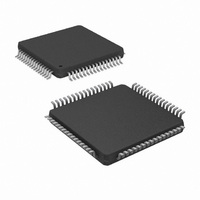
IC TXRX LVDS 9CH W/SCAN 64LQFP
Manufacturer
National Semiconductor
Series
SCANr
Type
Transceiverr
Datasheet
1.SCAN92LV090VEHNOPB.pdf
(14 pages)
Specifications of SCAN92LV090VEH/NOPB
Number Of Drivers/receivers
9/9
Protocol
IEEE 1149.1
Voltage - Supply
3 V ~ 3.6 V
Mounting Type
Surface Mount
Package / Case
64-LQFP
Lead Free Status / RoHS Status
Lead free / RoHS Compliant
Other names
*SCAN92LV090VEH
*SCAN92LV090VEH/NOPB
SCAN92LV090VEH
*SCAN92LV090VEH/NOPB
SCAN92LV090VEH
Available stocks
Company
Part Number
Manufacturer
Quantity
Price
Company:

Part Number:
SCAN92LV090VEH/NOPB
Manufacturer:
Texas Instruments
Quantity:
10 000


I
I
I
I
I
I
I
I
I
C
C
DIFFERENTIAL DRIVER TIMING REQUIREMENTS
t
t
t
t
t
t
t
t
t
t
t
DIFFERENTIAL RECEIVER TIMING REQUIREMENTS
IH
ILR
IL
CCD
CCR
CCZ
CC
CCS
OFF
PHLD
PLHD
SKD1
SKD2
SKD3
TLH
THL
PHZ
PLZ
PZH
PZL
Symbol
OUTPUT
OUTPUT
Symbol
AC Electrical Characteristics
Over recommended operating supply voltage and temperature ranges unless otherwise specified (Note 6)
Input High Current
Input Low Current
Input Low Current
Power Supply Current
Drivers Enabled, Receivers
Disabled
Power Supply Current
Drivers Disabled, Receivers
Enabled
Power Supply Current,
Drivers and Receivers TRI-
STATE
Power Supply Current,
Drivers and Receivers
Enabled
Power Supply Current
(SCAN Test Mode), Drivers
and Receivers Enabled
Power Off Leakage Current V
Capacitance @ Bus Pins
Capacitance @ R
Differential Prop. Delay High to Low (Note 8)
Differential Prop. Delay Low to High (Note 8)
Differential Skew |t
Chip to Chip Skew (Note 12)
Channel to Channel Skew (Note 13)
Transition Time Low to High
Transition Time High to Low
Disable Time High to Z
Disable Time Low to Z
Enable Time Z to High
Enable Time Z to Low
®
Parameter
OUT
PHLD
–t
Parameter
PLHD
V
V
VIN = GND
No Load, DE = RE = V
DIN = V
DE = RE = 0V, V
DE = 0V; RE = V
DIN = V
DE = V
DIN = V
R
DE = V
DIN = V
R
Test-Logic-Reset
D
V
IN
IN
L
L
CC
IN
APPLIED
| (Note 9)
= 27Ω
= 27Ω, TAP in any state other than
, DE, RE = 0V or OPEN,
= V
= GND, V
= 0V or OPEN,
CC
CC
CC
CC
CC
CC
CC
= 3.6V (Port Pins)
; RE = 0V,
; RE = 0V,
or GND
or GND
or GND,
or GND,
CC
Conditions
= 3.6v
ID
CC
= ±300mV
,
CC
,
5
R
Figure 2, Figure 3
C
R
Figure 4, Figure 5
C
L
L
L
L
= 27Ω,
= 10 pF
= 27Ω,
= 10 pF
Conditions
TDI, TMS,
TCK, TRST
TDI, TMS,
TRST
TCK
V
DO+/RI+,
DO−/RI−
DO+/RI+,
DO−/RI−
R
CC
OUT
Pin
Min
−20
-20
-25
-20
Min
1.0
1.0
Typ
160
180
50
50
50
5
7
0.25
Typ
120
1.8
1.8
0.5
0.5
3
3
3
3
Max
-115
www.national.com
+20
+20
210
230
+20
80
80
80
Max
0.55
2.6
2.6
1.6
1.2
1.2
8
8
8
8
Units
Unit
mA
mA
mA
mA
mA
µA
µA
µA
µA
pF
pF
ns
ns
ps
ns
ns
ns
ns
ns
ns
ns
ns
s
Related parts for SCAN92LV090VEH/NOPB
Image
Part Number
Description
Manufacturer
Datasheet
Request
R

Part Number:
Description:
National Semiconductor [8-Bit D/A Converter]
Manufacturer:
National Semiconductor
Datasheet:
Part Number:
Description:
National Semiconductor [Media Coprocessor]
Manufacturer:
National Semiconductor
Datasheet:
Part Number:
Description:
Digitally Controlled Tone and Volume Circuit with Stereo Audio Power Amplifier, Microphone Preamp Stage and National 3D Sound
Manufacturer:
National Semiconductor
Datasheet:
Part Number:
Description:
Digitally Controlled Tone and Volume Circuit with Stereo Audio Power Amplifier, Microphone Preamp Stage and National 3D Sound
Manufacturer:
National Semiconductor
Datasheet:
Part Number:
Description:
AC97 Rev 2 Codec with Sample Rate Conversion and National 3D Sound
Manufacturer:
National Semiconductor
Part Number:
Description:
Manufacturer:
National Semiconductor
Datasheet:
Part Number:
Description:
Manufacturer:
National Semiconductor
Datasheet:
Part Number:
Description:
General Purpose, Low Voltage, Low Power, Rail-to-Rail Output Operational Amplifiers
Manufacturer:
National Semiconductor
Datasheet:
Part Number:
Description:
8-bit 20 MSPS flash A/D converter.
Manufacturer:
National Semiconductor
Datasheet:
Part Number:
Description:
Low Noise Quad Operational Amplifier
Manufacturer:
National Semiconductor
Datasheet:
Part Number:
Description:
Quad Differential Line Receivers
Manufacturer:
National Semiconductor
Datasheet:
Part Number:
Description:
Quad High Speed Trapezoidal? Bus Transceiver
Manufacturer:
National Semiconductor
Datasheet:
Part Number:
Description:
Dual Line Receiver
Manufacturer:
National Semiconductor
Datasheet:
Part Number:
Description:
TTL to 10k ECL Level Translator with Latch
Manufacturer:
National Semiconductor
Datasheet: