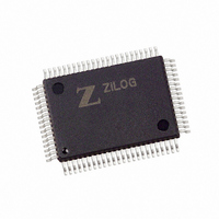
Z16C3220FSG Zilog, Z16C3220FSG Datasheet - Page 10

Z16C3220FSG
Manufacturer Part Number
Z16C3220FSG
Description
IC 20MHZ CMOS IUSC 80-QFP
Manufacturer
Zilog
Series
IUSC™r
Specifications of Z16C3220FSG
Controller Type
USC Controller
Interface
DMA
Voltage - Supply
4.5 V ~ 5.5 V
Current - Supply
7mA
Operating Temperature
0°C ~ 70°C
Mounting Type
Surface Mount
Package / Case
80-BQFP
Lead Free Status / RoHS Status
Lead free / RoHS Compliant
Available stocks
Company
Part Number
Manufacturer
Quantity
Price
PORT7/TxCOMPLT General-Purpose I/O or Transmit Com-
plete (input or output). Software can program the IUSC so
that this pin is a general-purpose input or output, or so that
it carries a Transmit Complete signal from the Transmitter,
that can control an external driver. The IUSC captures
transitions on this pin in internal latches.
PORT6/FSYNC General-Purpose I/O or Frame Sync (in-
put or output). Software can program the IUSC so that this
pin is a general-purpose input or output, or a Frame Sync
input for the IUSC’s Time Slot Assigner circuits. The IUSC
captures transitions on this pin in internal latches.
PORT5/RxSYNC General-Purpose I/O or Receive Sync
(input or output). Software can program the IUSC so that
this pin is a general-purpose input or output, or so that it
carries a Receive Sync output from the Receiver. The IUSC
captures transitions on this pin in internal latches.
PORT4/TxTSA General-Purpose I/O or Transmit Time Slot
Assigner Gate (input or output). Software can program the
IUSC so that this pin is a general-purpose input or output,
or so that it carries the Gate output of the Transmit Time Slot
Assigner, that can enable an external TxD driver in time-
slotted ISDN or Fractional T1 applications. The IUSC
captures transitions on this pin in internal latches, as
described in the text.
ARCHITECTURE
The IUSC integrates a fast and efficient dual-channel DMA
with a highly versatile serial communications controller.
The functional capabilities of the IUSC are described from
two different points of view; as a datacommunications
device, it transmits and receives data in a wide variety of
datacommunications protocols; as a microprocessor pe-
ripheral with two DMA channels that offer such features as
Z
PS97USC0200
ILOG
P R E L I M I N A R Y
PORT 3/RxTSA General-Purpose I/O or Receive Time Slot
Assigner Gate (input or output). Software can program the
IUSC so that this pin is a general-purpose input or output,
or so that it carries the Gate output of the Receive Time Slot
Assigner. The IUSC captures transitions on this pin in
internal latches.
PORT 2 General-Purpose I/O (input or output). Software
can program the IUSC so that this pin is a general-purpose
input or output. The IUSC captures transitions on this pin
in internal latches.
PORT 1-0/CLK 1-0 General-Purpose I/Os or Reference
Clocks (inputs or outputs). Software can program the IUSC
so that either of these pins is a general-purpose input or
output, or a reference clock that can be divided down to
derive clocking for the Receiver and/or Transmitter. When
one of these pins is a general-purpose I/O, the IUSC
captures transitions on it in internal latches.
V
each power rail ensures good signal integrity, prevents
transients on outputs, and improves noise margins on
inputs. The IUSC’s internal power distribution network
requires that all these pins be connected appropriately.
four DMA transfer types, a flexible bus interface, and
vectored interrupts. The architecture is described in three
sections, DMA and Bus Interface Capabilities, Communi-
cation between the DMA and Serial Channel, and Serial
Communication Capabilities. The structure of the IUSC is
shown in Figure 1.
CC
, V
SS
Power and Ground. The inclusion of seven pins for
Z16C32 IUSC
10
™


