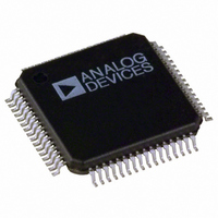
ADV7202KST Analog Devices Inc, ADV7202KST Datasheet - Page 24

ADV7202KST
Manufacturer Part Number
ADV7202KST
Description
IC CODEC VIDEO 10BIT 64LQFP
Manufacturer
Analog Devices Inc
Type
Video Codecr
Datasheet
1.ADV7202KSTZ.pdf
(28 pages)
Specifications of ADV7202KST
Rohs Status
RoHS non-compliant
Data Interface
Serial
Resolution (bits)
12, 10 b
Number Of Adcs / Dacs
1 / 4
Sigma Delta
No
Voltage - Supply, Analog
4.75 V ~ 5.25 V
Voltage - Supply, Digital
4.75 V ~ 5.25 V
Operating Temperature
0°C ~ 70°C
Mounting Type
Surface Mount
Package / Case
64-LQFP
Lead Free Status / Rohs Status
Not Compliant
Available stocks
Company
Part Number
Manufacturer
Quantity
Price
Company:
Part Number:
ADV7202KST
Manufacturer:
CSR
Quantity:
1 000
Company:
Part Number:
ADV7202KSTZ
Manufacturer:
Analog Devices Inc
Quantity:
10 000
ADV7202
CLAMP CONTROL
The clamp control has two modes of operation, if the synchronize
clamp control bit CR16 (Bit-6 address 07h) is set, then the clamps
that are enabled will be switched on for the programmed time when
triggered by the Sync_IN control signal, this control signal is edge
detected and its polarity can be set by MR35 (Bit 5 Address 03h).
If the synchronize clamp control bit is set to zero, when enabled
each clamp will switch on for the programmed time. The clamp
control bits are edge detected and the bits must first be reset to
zero before the clamps can be switched on again.
DAC TERMINATION AND LAYOUT CONSIDERATIONS
Resistor R
and is used to control the amplitude of the DAC output current.
Therefore, a recommended RSET value of 1200 Ω will enable an
I
value of 300 Ω.
The ADV7202 has four analog outputs—DAC0, DAC1, DAC2,
and DAC3. For cable driving the DACs should be used with an
external buffer. Suitable op amps are the AD8057 or AD8061.
PC BOARD LAYOUT CONSIDERATIONS
The ADV7202 is optimally designed for the lowest noise perfor-
mance, both radiated and conducted noise. To complement the
excellent noise performance of the ADV7202, it is imperative
that great care be given to the PC board layout.
The layout should be optimized for lowest noise on the ADV7202
power and ground lines. This can be achieved by shielding the
digital inputs and providing good decoupling. The lead length
between groups of AVDD, AVSS, DVDD, and DVSS pins
should be kept as short as possible to minimize inductive ringing.
It is recommended that a four-layer printed circuit board be
used, with power and ground planes separating the layer of the
signal carrying traces of the components and solder side layer.
Placement of components should be considered to separate noisy
circuits, such as crystal clocks, high speed logic circuitry, and
analog circuitry.
There should be separate analog and digital ground planes
(AVSS and DVSS).
MAX
I
MAX
of 4.43 mA. V
= 5 196
SET
.
is connected between the RSET pin and AVSS
R
SET
MAX
Amps
= R
LOAD
× I
MAX
, R
LOAD
should have a
(3)
–24–
Power planes should encompass a digital power plane (DVDD)
and an analog power plane (AVDD). The analog power plane
should contain the ADCs and all associated circuitry, includ-
ing VREF circuitry. The digital power plane should contain all
logic circuitry. The analog and digital power planes should be
individually connected to the common power plane at one single
point through a suitable filtering device such as a ferrite bead.
DAC output traces on a PCB should be treated as transmission
lines. It is recommended that the DACs be placed as close as pos-
sible to the output connector, with the analog output traces being
as short as possible (less than three inches). The DAC termination
resistors should be placed as close as possible to the DAC outputs
and should overlay the PCB’s ground plane. As well as minimizing
reflections, short analog output traces will reduce noise pickup
due to neighboring digital circuitry.
Supply Decoupling
Noise on the analog power plane can be further reduced by the
use of decoupling capacitors.
Optimum performance is achieved by the use of 0.1 µF ceramic
capacitors. Each of the group of AVDD or DVDD pins should be
individually decoupled to ground. This should be done by placing
the capacitors as close as possible to the device with the capacitor
leads as short as possible, thus minimizing lead inductance.
Digital Signal Interconnect
The digital signal lines should be isolated as much as possible from
the analog outputs and other analog circuitry. Digital signal lines
should not overlay the analog power plane.
Due to the high clock rates used, long clock lines to the ADV7202
should be avoided to minimize noise pickup.
Any active pull-up termination resistors for the digital inputs
should be connected to the digital power plane and not the analog
power plane.
Analog Signal Interconnect
The ADV7202 should be located as close as possible to the output
connectors, thus minimizing noise pickup and reflections due to
impedance mismatch.
For optimum performance, the analog outputs should each be
source and load terminated, as shown in Figure 35. The termination
resistors should be as close as possible to the ADV7202 to minimize
reflections.
Any unused inputs should be tied to the ground.
REV. 0


