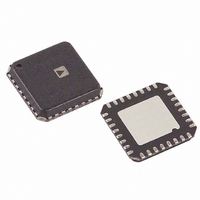
ADAU1361BCPZ Analog Devices Inc, ADAU1361BCPZ Datasheet - Page 41

ADAU1361BCPZ
Manufacturer Part Number
ADAU1361BCPZ
Description
IC CODEC 24B PLL 32LFCSP
Manufacturer
Analog Devices Inc
Type
Audio Codecr
Datasheet
1.ADAU1361BCPZ-RL.pdf
(80 pages)
Specifications of ADAU1361BCPZ
Data Interface
Serial
Resolution (bits)
24 b
Number Of Adcs / Dacs
2 / 2
Sigma Delta
No
Voltage - Supply, Analog
1.8 V ~ 3.6 V
Voltage - Supply, Digital
1.8 V ~ 3.6 V
Operating Temperature
-40°C ~ 85°C
Mounting Type
Surface Mount
Package / Case
32-VFQFN, CSP Exposed Pad
Audio Codec Type
Stereo
No. Of Adcs
2
No. Of Dacs
2
No. Of Input Channels
6
No. Of Output Channels
7
Adc / Dac Resolution
24bit
Adcs / Dacs Signal To Noise Ratio
101dB
Lead Free Status / RoHS Status
Lead free / RoHS Compliant
Available stocks
Company
Part Number
Manufacturer
Quantity
Price
Company:
Part Number:
ADAU1361BCPZ
Manufacturer:
TOSHIBA
Quantity:
1 650
Company:
Part Number:
ADAU1361BCPZ
Manufacturer:
ADI
Quantity:
624
Part Number:
ADAU1361BCPZ
Manufacturer:
ADI/亚德诺
Quantity:
20 000
Part Number:
ADAU1361BCPZ-R7
Manufacturer:
ADI/亚德诺
Quantity:
20 000
SPI PORT
By default, the ADAU1361 is in I
SPI control mode by pulling CLATCH low three times. This is
done by performing three dummy writes to the SPI port (the
ADAU1361 does not acknowledge these three writes). Beginning
with the fourth SPI write, data can be written to or read from
the IC. The ADAU1361 can be taken out of SPI mode only by
a full reset initiated by power-cycling the IC.
The SPI port uses a 4-wire interface, consisting of the CLATCH ,
CCLK, CDATA, and COUT signals, and it is always a slave port.
The CLATCH signal should go low at the beginning of a trans-
action and high at the end of a transaction. The CCLK signal
latches CDATA on a low-to-high transition. COUT data is shifted
out of the ADAU1361 on the falling edge of CCLK and should
be clocked into a receiving device, such as a microcontroller, on
the CCLK rising edge. The CDATA signal carries the serial input
data, and the COUT signal carries the serial output data. The
COUT signal remains three-state until a read operation is requested.
This allows other SPI-compatible peripherals to share the same
readback line. All SPI transactions have the same basic format
shown in
data should be written MSB first.
Table 23. Generic Control Word Format
Byte 0
chip_adr[6:0], R/W
1
Continues to end of data.
Table 23
CLATCH
CDATA
CCLK
CLATCH
CDATA
. A timing diagram is shown in
COUT
CCLK
Byte 1
subaddr[15:8]
2
BYTE 0
C mode, but it can be put into
HIGH-Z
Figure 55. SPI Read from ADAU1361 Clocking (Single-Word Read Mode)
Figure 54. SPI Write to ADAU1361 Clocking (Single-Word Write Mode)
BYTE 0
Figure 4
BYTE 1
Byte 2
subaddr[7:0]
. All
Rev. C | Page 41 of 80
BYTE 2
Chip Address R/ W
The LSB of the first byte of an SPI transaction is a R/ W bit. This bit
determines whether the communication is a read (Logic Level 1)
or a write (Logic Level 0). This format is shown in
Table 22. ADAU1361 SPI Address and Read/ Write Byte Format
Bit 0
0
Subaddress
The 16-bit subaddress word is decoded into a location in one of
the registers. This subaddress is the location of the appropriate
register. The MSBs of the subaddress are zero-padded to bring
the word to a full 2-byte length.
Data Bytes
The number of data bytes varies according to the register being
accessed. During a burst mode write, an initial subaddress is
written followed by a continuous sequence of data for consecu-
tive register locations.
A sample timing diagram for a single-word SPI write operation
to a register is shown in Figure 54. A sample timing diagram of
a single-word SPI read operation is shown in Figure 55. The
COUT pin goes from being three-state to being driven at the
beginning of Byte 3. In this example, Byte 0 to Byte 2 contain
the addresses and R/ W bit, and subsequent bytes carry the data.
BYTE 1
Bit 1
0
Byte 3
data
DATA
Bit 2
0
BYTE 2
Bit 3
0
Bit 4
0
BYTE 3
Byte 4
data
HIGH-Z
Bit 5
0
1
ADAU1361
Bit 6
0
Table 22
.
Bit 7
R/W


