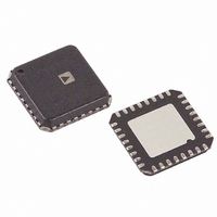
ADAU1361BCPZ Analog Devices Inc, ADAU1361BCPZ Datasheet - Page 16

ADAU1361BCPZ
Manufacturer Part Number
ADAU1361BCPZ
Description
IC CODEC 24B PLL 32LFCSP
Manufacturer
Analog Devices Inc
Type
Audio Codecr
Datasheet
1.ADAU1361BCPZ-RL.pdf
(80 pages)
Specifications of ADAU1361BCPZ
Data Interface
Serial
Resolution (bits)
24 b
Number Of Adcs / Dacs
2 / 2
Sigma Delta
No
Voltage - Supply, Analog
1.8 V ~ 3.6 V
Voltage - Supply, Digital
1.8 V ~ 3.6 V
Operating Temperature
-40°C ~ 85°C
Mounting Type
Surface Mount
Package / Case
32-VFQFN, CSP Exposed Pad
Audio Codec Type
Stereo
No. Of Adcs
2
No. Of Dacs
2
No. Of Input Channels
6
No. Of Output Channels
7
Adc / Dac Resolution
24bit
Adcs / Dacs Signal To Noise Ratio
101dB
Lead Free Status / RoHS Status
Lead free / RoHS Compliant
Available stocks
Company
Part Number
Manufacturer
Quantity
Price
Company:
Part Number:
ADAU1361BCPZ
Manufacturer:
TOSHIBA
Quantity:
1 650
Company:
Part Number:
ADAU1361BCPZ
Manufacturer:
ADI
Quantity:
624
Part Number:
ADAU1361BCPZ
Manufacturer:
ADI/亚德诺
Quantity:
20 000
Part Number:
ADAU1361BCPZ-R7
Manufacturer:
ADI/亚德诺
Quantity:
20 000
ADAU1361
Pin No.
19
20
21
22
23
24
25
26
27
28
29
30
31
32
EP
1
A_IN = analog input, A_OUT = analog output, D_IN = digital input, D_IO = digital input/output, D_OUT = digital output, PWR = power.
Mnemonic
RHP
LHP
MONOOUT
AGND
AVDD
DVDDOUT
DGND
ADC_SDATA
DAC_SDATA
BCLK
LRCLK
ADDR1/CDATA
SDA/COUT
SCL/CCLK
Exposed Pad
Type
A_OUT
A_OUT
A_OUT
PWR
PWR
PWR
D_IN
D_IO
D_IO
D_IN
D_IO
PWR
D_OUT
D_IN
1
Description
Right Headphone Output. Biased at AVDD/2.
Left Headphone Output. Biased at AVDD/2.
Mono Output or Virtual Ground for Capless Headphone. Biased at AVDD/2 when set as mono
output.
Analog Ground. The AGND and DGND pins can be tied together on a common ground plane.
AGND should be decoupled locally to AVDD with a 100 nF capacitor.
1.8 V to 3.3 V Analog Supply for ADC, Output Driver, and Input to Digital Supply Regulator.
This pin should be decoupled locally to AGND with a 100 nF capacitor.
Digital Core Supply Decoupling Point. The digital supply is generated from an on-board
regulator and does not require an external supply. DVDDOUT should be decoupled to DGND
with a 100 nF capacitor and a 10 μF capacitor.
Digital Ground. The AGND and DGND pins can be tied together on a common ground plane.
DGND should be decoupled to DVDDOUT and to IOVDD with 100 nF capacitors and 10 μF
capacitors.
ADC Serial Output Data.
DAC Serial Input Data.
Serial Data Port Bit Clock.
Serial Data Port Frame Clock.
I
SPI Data Input (CDATA).
I
this pin should have a 2 kΩ pull-up resistor.
SPI Data Output (COUT). This pin is used for reading back registers and memory locations. It is
three-state when an SPI read is not active.
I
connected to this pin should have a 2 kΩ pull-up resistor.
SPI Clock (CCLK). This pin can run continuously or be gated off between SPI transactions.
Exposed Pad. The exposed pad is connected internally to the ADAU1361 grounds. For
increased reliability of the solder joints and maximum thermal capability, it is recommended
that the pad be soldered to the ground plane. See the Exposed Pad PCB Design section for
more information.
2
2
2
C Address Bit 1 (ADDR1).
C Data (SDA). This pin is a bidirectional open-collector input/output. The line connected to
C Clock (SCL). This pin is always an open-collector input when in I
Rev. C | Page 16 of 80
2
C control mode. The line


