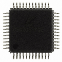
CS4205-KQZ Cirrus Logic Inc, CS4205-KQZ Datasheet - Page 41

CS4205-KQZ
Manufacturer Part Number
CS4205-KQZ
Description
IC CODEC AC97 I2S 48-LQFP
Manufacturer
Cirrus Logic Inc
Type
Audio Codec '97r
Datasheet
1.CS4205-KQZ.pdf
(81 pages)
Specifications of CS4205-KQZ
Package / Case
48-LQFP
Data Interface
Serial
Resolution (bits)
18, 20 b
Number Of Adcs / Dacs
1 / 2
Sigma Delta
Yes
Dynamic Range, Adcs / Dacs (db) Typ
90 / 90
Voltage - Supply, Analog
4.75 V ~ 5.25 V
Voltage - Supply, Digital
4.75 V ~ 5.25 V
Operating Temperature
0°C ~ 70°C
Mounting Type
Surface Mount
Number Of Adc Inputs
8
Number Of Dac Outputs
3
Conversion Rate
48 KSPs
Interface Type
Serial (5-Wire)
Resolution
18 bit, 20 bit
Maximum Operating Temperature
+ 70 C
Mounting Style
SMD/SMT
Minimum Operating Temperature
0 C
Number Of Channels
1 ADC, 1 DAC
Lead Free Status / RoHS Status
Lead free / RoHS Compliant
Other names
598-1182
Available stocks
Company
Part Number
Manufacturer
Quantity
Price
Company:
Part Number:
CS4205-KQZ
Manufacturer:
Vishay
Quantity:
718
Company:
Part Number:
CS4205-KQZR
Manufacturer:
Cirrus Logic Inc
Quantity:
10 000
5.23
GW[4:0]
Default
GPIO bits which have been programmed as inputs, “sticky”, and “wakeup”, upon transition either (high-to-low) or
(low-to-high) depending on pin polarity, will cause an AC-link wakeup if and only if the AC-link was powered down.
Once the controller has re-established communication with the CS4205 following a Warm Reset, it will continue to
signal the wakeup event through the GPIO_INT bit of input Slot 12 until the AC ’97 controller clears the inter-
rupt-causing bit in the GPIO Pin Status Register (Index 54h); or the “wakeup”, config, or “sticky” status of that GPIO
pin changes.
After a Cold Reset or a modem Register Reset (see Extended Modem ID Register (Index 3Ch)) this register defaults
to all 0’s, specifying no wakeup event. The upper 11 bits of this register always return ‘0’.
5.24
GI[4:0]
Default
GPIO pins which have been programmed as inputs and “sticky”, upon transition either (high-to-low) or (low-to-high)
depending on pin polarity, will cause the individual GI bit to be ‘set’, and remain ‘set’ until ‘cleared’. GPIO pins which
have been programmed as outputs are controlled either through output Slot 12 or through this register, depending
on the state of the GPOC bit in the Misc. Crystal Control Register (Index 60h). If the GPOC bit is ‘cleared’, the GI
bits in this register are read-only and reflect the status of the corresponding GPIO output pin ‘set’ through output
slot 12. If the GPOC bit is ‘set’, the GI bits in this register are read/write bits and control the corresponding GPIO
output pins.
The default value is always the state of the GPIO pin. The upper 11 bits of this register should be forced to zero in
this register and input Slot 12.
5.25
DACS
DS489PP4
DACS CAPS1 CAPS0 MICS
D15
D15
D15
0
0
GPIO Pin Wakeup Mask Register (Index 52h)
GPIO Pin Status Register (Index 54h)
AC Mode Control Register (Index 5Eh)
D14
D14
D14
0
0
D13
D13
D13
0
0
GPIO Pin Status. This register reflects the state of all GPIO pin inputs and outputs. These
values are also reflected in Slot 12 of every SDATA_IN frame. GPIO inputs configured as
“sticky” are ‘cleared’ by writing a ‘0’ to the corresponding bit of this register. The GPIO_INT
bit in input Slot 12 is ‘cleared’ by clearing all interrupt-causing bits in this register.
0000h
is ‘clear’, the DACs will receive data from the DAC slots, see Table 14 for actual slots used.
If this bit is ‘set’, the DACs will receive data from the CS4205 digital effects engine.
GPIO Pin Wakeup. This register provides a mask for determining if an input GPIO change will
generate a wakeup event (0 = no, 1 = yes). When the AC-link is powered up, a wakeup event
will be communicated through the assertion of GPIO_INT = 1 in input Slot 12. When the
AC-link is powered down (Powerdown Control/Status Register (Index 26h) bit PR4 = 1 for pri-
mary codecs), a wakeup event will be communicated through a ‘0’ to ‘1’ transition on
SDATA_IN.
0000h
DAC Source Select. The DACS bit controls the source of data routed to the DACs. If this bit
D12
D12
D12
0
0
D11
D11
D11
0
0
0
D10
D10
D10
0
0
0
TMM
D9
D9
D9
0
0
DDM AMAP
D8
D8
D8
0
0
D7
D7
D7
0
0
D6
D6
D6
0
0
0
SM1
D5
D5
D5
0
0
SM0 SDOS1 SDOS0 SPDS1 SPDS0
GW4
D4
GI4
D4
D4
GW3
D3
GI3
D3
D3
GW2
GI2
D2
D2
D2
GW1
CS4205
GI1
D1
D1
D1
GW0
GI0
D0
D0
D0
41


