CS42L52-CNZ Cirrus Logic Inc, CS42L52-CNZ Datasheet - Page 7
CS42L52-CNZ
Manufacturer Part Number
CS42L52-CNZ
Description
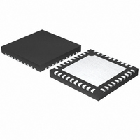
IC CODEC STER HDPN & SPKR 40QFN
Manufacturer
Cirrus Logic Inc
Type
Stereo Audior
Datasheet
1.CS42L52-CNZ.pdf
(82 pages)
Specifications of CS42L52-CNZ
Package / Case
40-QFN
Data Interface
Serial
Resolution (bits)
24 b
Number Of Adcs / Dacs
1 / 1
Sigma Delta
Yes
Dynamic Range, Adcs / Dacs (db) Typ
99 / 98
Voltage - Supply, Analog
1.65 V ~ 2.63 V
Voltage - Supply, Digital
1.65 V ~ 2.63 V
Operating Temperature
-40°C ~ 85°C
Mounting Type
Surface Mount
Number Of Adc Inputs
8
Number Of Dac Outputs
2
Conversion Rate
96 KSPS
Interface Type
Serial (I2C)
Resolution
24 bit
Maximum Operating Temperature
+ 85 C
Mounting Style
SMD/SMT
Minimum Operating Temperature
- 40 C
Number Of Channels
2 ADC/2 DAC
Thd Plus Noise
- 88 dB ADC / - 86 dB DAC
Package
40QFN EP
Adc/dac Resolution
24 Bit
Sampling Rate
96 KSPS
Number Of Dacs
2
Operating Supply Voltage
2.5 V
Lead Free Status / RoHS Status
Lead free / RoHS Compliant
For Use With
598-1580 - REFERENCE DESIGN FOR CS42L52598-1508 - BOARD EVAL FOR 42LDB1 CODEC598-1505 - BOARD EVAL FOR CS42L52 CODEC
Lead Free Status / Rohs Status
Lead free / RoHS Compliant
Other names
598-1628
Available stocks
Company
Part Number
Manufacturer
Quantity
Price
Company:

Part Number:
CS42L52-CNZ
Manufacturer:
CIRRUS
Quantity:
441
Part Number:
CS42L52-CNZ
Manufacturer:
CIRRUS
Quantity:
20 000
Company:
Part Number:
CS42L52-CNZR
Manufacturer:
MINI
Quantity:
2 300
Part Number:
CS42L52-CNZR
Manufacturer:
CIRRUS
Quantity:
20 000


DS680F1
LIST OF FIGURES
9. PCB LAYOUT CONSIDERATIONS ..................................................................................................... 77
10. ADC & DAC DIGITAL FILTERS ........................................................................................................ 78
11. PARAMETER DEFINITIONS .............................................................................................................. 79
12. PACKAGE DIMENSIONS .................................................................................................................. 80
13. ORDERING INFORMATION .............................................................................................................. 81
14. REFERENCES .................................................................................................................................... 81
15. REVISION HISTORY .......................................................................................................................... 81
Figure 1. Typical Connection Diagram ...................................................................................................... 10
Figure 2. Headphone Output Test Load .................................................................................................... 19
Figure 3. Serial Audio Interface Timing ..................................................................................................... 21
Figure 4. Control Port Timing - I²C ............................................................................................................ 22
Figure 5. Analog Input Signal Flow ........................................................................................................... 26
Figure 6. Single-Ended MIC Configuration ............................................................................................... 27
Figure 7. Differential MIC Configuration .................................................................................................... 27
Figure 8. ALC ............................................................................................................................................ 28
Figure 9. Noise Gate Attenuation .............................................................................................................. 28
Figure 10. DSP Engine Signal Flow .......................................................................................................... 29
Figure 11. PWM Output Stage .................................................................................................................. 30
Figure 12. Analog Output Stage ................................................................................................................ 30
Figure 13. Beep Configuration Options ..................................................................................................... 31
Figure 14. Peak Detect & Limiter .............................................................................................................. 32
Figure 15. Battery Compensation ............................................................................................................. 34
Figure 16. I²S Format ................................................................................................................................ 36
Figure 17. Left-Justified Format ................................................................................................................ 36
Figure 18. Right-Justified Format (DAC only) ........................................................................................... 36
Figure 19. DSP Mode Format) .................................................................................................................. 36
Figure 20. Control Port Timing, I²C Write .................................................................................................. 38
Figure 21. Control Port Timing, I²C Read .................................................................................................. 38
Figure 22. THD+N vs. Output Power per Channel at 1.8 V (16 Ω load) ................................................... 74
Figure 23. THD+N vs. Output Power per Channel at 2.5 V (16 Ω load) ................................................... 74
Figure 24. THD+N vs. Output Power per Channel at 1.8 V (32 Ω load) ................................................... 75
Figure 25. THD+N vs. Output Power per Channel at 2.5 V (32 Ω load) ................................................... 75
Figure 26. ADC Passband Ripple ............................................................................................................. 78
Figure 27. ADC Stopband Rejection ......................................................................................................... 78
Figure 28. ADC Transition Band ............................................................................................................... 78
Figure 29. ADC Transition Band (Detail) ................................................................................................... 78
Figure 30. DAC Passband Ripple ............................................................................................................. 78
Figure 31. DAC Stopband ......................................................................................................................... 78
Figure 32. DAC Transition Band ............................................................................................................... 78
Figure 33. DAC Transition Band (Detail) ................................................................................................... 78
THERMAL CHARACTERISTICS .......................................................................................................... 80
8.2 Auto Detect Disabled ...................................................................................................................... 76
9.1 Power Supply, Grounding ............................................................................................................... 77
9.2 QFN Thermal Pad .......................................................................................................................... 77
5/13/08
CS42L52
7
Related parts for CS42L52-CNZ
Image
Part Number
Description
Manufacturer
Datasheet
Request
R

Part Number:
Description:
IC,Soundcard Circuits,LLCC,40PIN,PLASTIC
Manufacturer:
Cirrus Logic Inc
Datasheet:
Part Number:
Description:
IC,Soundcard Circuits,LLCC,40PIN,PLASTIC
Manufacturer:
Cirrus Logic Inc
Datasheet:
Part Number:
Description:
IC,Soundcard Circuits,LLCC,40PIN,PLASTIC
Manufacturer:
Cirrus Logic Inc
Datasheet:

Part Number:
Description:
Development Kit
Manufacturer:
Cirrus Logic Inc
Datasheet:
Part Number:
Description:
Development Kit
Manufacturer:
Cirrus Logic Inc
Datasheet:


Part Number:
Description:
High-efficiency PFC + Fluorescent Lamp Driver Reference Design
Manufacturer:
Cirrus Logic Inc
Datasheet:
Part Number:
Description:
Development Kit
Manufacturer:
Cirrus Logic Inc
Datasheet:
Part Number:
Description:
Development Kit
Manufacturer:
Cirrus Logic Inc
Datasheet:

Part Number:
Description:
Development Kit
Manufacturer:
Cirrus Logic Inc
Datasheet:
Part Number:
Description:
Development Kit
Manufacturer:
Cirrus Logic Inc
Datasheet:
Part Number:
Description:
Development Kit
Manufacturer:
Cirrus Logic Inc
Datasheet:
Part Number:
Description:
Development Kit
Manufacturer:
Cirrus Logic Inc
Datasheet:

Part Number:
Description:
Ref Bd For Speakerbar MSA & DSP Products
Manufacturer:
Cirrus Logic Inc