MPC8315ECVRAGDA Freescale Semiconductor, MPC8315ECVRAGDA Datasheet - Page 79
MPC8315ECVRAGDA
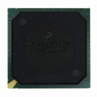
Manufacturer Part Number
MPC8315ECVRAGDA
Description
MPU POWERQUICC II PRO 620-PBGA
Manufacturer
Freescale Semiconductor
Datasheet
1.MPC8315VRADDA.pdf
(112 pages)
Specifications of MPC8315ECVRAGDA
Processor Type
MPC83xx PowerQUICC II Pro 32-Bit
Speed
400MHz
Voltage
1V
Mounting Type
Surface Mount
Package / Case
620-PBGA
Processor Series
MPC8xxx
Core
e300
Data Bus Width
32 bit
Maximum Clock Frequency
50 MHz
Maximum Operating Temperature
+ 105 C
Mounting Style
SMD/SMT
Minimum Operating Temperature
- 40 C
Leaded Process Compatible
Yes
Rohs Compliant
Yes
Peak Reflow Compatible (260 C)
Yes
Lead Free Status / RoHS Status
Lead free / RoHS Compliant
Features
-
Lead Free Status / Rohs Status
Lead free / RoHS Compliant
Available stocks
Company
Part Number
Manufacturer
Quantity
Price
Company:

Part Number:
MPC8315ECVRAGDA
Manufacturer:
Freescale Semiconductor
Quantity:
135
Company:
Part Number:
MPC8315ECVRAGDA
Manufacturer:
FREESCAL
Quantity:
36
Company:
Part Number:
MPC8315ECVRAGDA
Manufacturer:
Freescale Semiconductor
Quantity:
10 000
Part Number:
MPC8315ECVRAGDA
Manufacturer:
FREESCALE
Quantity:
20 000


Figure 51
Freescale Semiconductor
TDMxTFS/TDMxRFS input hold time
TDMxTCK High to TDMxTD output active
TDMxTCK High to TDMxTD output valid
TDMxTD hold time
TDMxTCK High to TDMxTD output high impedance
TDMxTFS/TDMxRFS output valid
TDMxTFS/TDMxRFS output hold time
Notes:
1. The symbols used for timing specifications herein follow the pattern of t
2. Output values are based on 30 pF capacitive load.
3. Inputs are referenced to the sampling that the TDM is programmed to use. Outputs are referenced to the programming edge
for inputs and t
timing (DM) with respect to the time the input signals (I) reach the valid state (V) relative to the TDM Clock, t
going to the high (H) state or setup time. Also, output signals (O), hold (X).
they are programmed to use. Use of the rising edge or falling edge as a reference is programmable. TDMxTCK and TDMxRCK
are shown using the rising edge.
shows the TDM receive signal timing.
(first two letters of functional block)(reference)(state)(signal)(state)
Parameter/Condition
TDMxRFS (output)
MPC8315E PowerQUICC
TDMxRCK
TDMxRFS
TDMxRD
t
t
DMIVKH
DMIVKH
Table 69. TDM AC Timing specifications
Figure 59. TDM Receive Signals
™
II Pro Processor Hardware Specifications, Rev. 0
t
DM_HIGH
t
t
DMRDIXKH
DMFSIXKH
t
t
t
t
t
t
t
DMFSKHOV
DM_OUTAC
DMFSKHOX
DMFSIXKH
DM_OUTHI
DMTKHOV
Symbol
DMTKHOX
t
DM
t
DMFSKHOV
for outputs. For example, t
(first two letters of functional block)(signal)(state) (reference)(state)
t
DM_LOW
Min
2.0
4.0
2.0
2.5
—
—
—
TDMIVKH
Max
14.0
10.0
13.5
—
—
—
—
t
DMFSKHOX
symbolizes TDM
TC
, reference (K)
Units
ns
ns
ns
ns
ns
ns
ns
TDM
79
Related parts for MPC8315ECVRAGDA
Image
Part Number
Description
Manufacturer
Datasheet
Request
R

Part Number:
Description:
BOARD MPU 8315 POWERQUICC II
Manufacturer:
Freescale Semiconductor
Datasheet:

Part Number:
Description:
PROCESSOR BOARD PWRQUICCII PBGA
Manufacturer:
Freescale Semiconductor
Datasheet:
Part Number:
Description:
PowerQUICC II Pro Processor Hardware Specifications
Manufacturer:
Freescale Semiconductor

Part Number:
Description:
Manufacturer:
Freescale Semiconductor, Inc
Datasheet:
Part Number:
Description:
Manufacturer:
Freescale Semiconductor, Inc
Datasheet:
Part Number:
Description:
Manufacturer:
Freescale Semiconductor, Inc
Datasheet:
Part Number:
Description:
Manufacturer:
Freescale Semiconductor, Inc
Datasheet:
Part Number:
Description:
Manufacturer:
Freescale Semiconductor, Inc
Datasheet:
Part Number:
Description:
Manufacturer:
Freescale Semiconductor, Inc
Datasheet:
Part Number:
Description:
Manufacturer:
Freescale Semiconductor, Inc
Datasheet:
Part Number:
Description:
Manufacturer:
Freescale Semiconductor, Inc
Datasheet:
Part Number:
Description:
Manufacturer:
Freescale Semiconductor, Inc
Datasheet:
Part Number:
Description:
Manufacturer:
Freescale Semiconductor, Inc
Datasheet:
Part Number:
Description:
Manufacturer:
Freescale Semiconductor, Inc
Datasheet:
Part Number:
Description:
Manufacturer:
Freescale Semiconductor, Inc
Datasheet: