ADSP-2101BS-100 Analog Devices Inc, ADSP-2101BS-100 Datasheet - Page 44
ADSP-2101BS-100
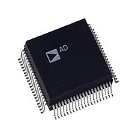
Manufacturer Part Number
ADSP-2101BS-100
Description
IC DSP CONTROLLER 16BIT 80PQFP
Manufacturer
Analog Devices Inc
Series
ADSP-21xxr
Type
Fixed Pointr
Datasheet
1.ADSP-2115BPZ-100.pdf
(64 pages)
Specifications of ADSP-2101BS-100
Rohs Status
RoHS non-compliant
Interface
Synchronous Serial Port (SSP)
Clock Rate
25MHz
Non-volatile Memory
External
On-chip Ram
6kB
Voltage - I/o
5.00V
Voltage - Core
5.00V
Operating Temperature
-40°C ~ 85°C
Mounting Type
Surface Mount
Package / Case
80-MQFP, 80-PQFP
Device Core Size
16b
Architecture
Enhanced Harvard
Format
Fixed Point
Clock Freq (max)
25MHz
Mips
25
Device Input Clock Speed
25MHz
Ram Size
3KB
Program Memory Size
Not RequiredKB
Operating Supply Voltage (typ)
5V
Operating Supply Voltage (min)
4.5V
Operating Supply Voltage (max)
5.5V
Operating Temp Range
-40C to 85C
Operating Temperature Classification
Industrial
Mounting
Surface Mount
Pin Count
80
Package Type
PQFP
Lead Free Status / Rohs Status
Not Compliant
Available stocks
Company
Part Number
Manufacturer
Quantity
Price


ADSP-21xx
TIMING PARAMETERS (ADSP-2103/2162/2164)
GENERAL NOTES
Use the exact timing information given. Do not attempt to
derive parameters from the addition or subtraction of others.
While addition or subtraction would yield meaningful results for
an individual device, the values given in this data sheet reflect
statistical variations and worst cases. Consequently, you cannot
meaningfully add parameters to derive longer times.
TIMING NOTES
Switching characteristics specify how the processor changes its
signals. You have no control over this timing—circuitry external
to the processor must be designed for compatibility with these
signal characteristics. Switching characteristics tell you what the
processor will do in a given circumstance. You can also use
switching characteristics to ensure that any timing requirement
of a device connected to the processor (such as memory) is
satisfied.
Memory Specification
Address Setup to Write Start
Address Setup to Write End
Address Hold Time
Data Setup Time
Data Hold Time
OE to Data Valid
Address Access Time
ADSP-21xx
Timing Parameter
t
t
t
t
t
t
t
ASW
AW
WRA
DW
DH
RDD
AA
–44–
Timing requirements apply to signals that are controlled by
circuitry external to the processor, such as the data input for a
read operation. Timing requirements guarantee that the
processor operates correctly with other devices.
MEMORY REQUIREMENTS
The table below shows common memory device specifications
and the corresponding ADSP-21xx timing parameters, for your
convenience.
Timing Parameter Definition
A0–A13, DMS, PMS Setup before WR Low
A0–A13, DMS, PMS Setup before WR Deasserted
A0–A13, DMS, PMS Hold after WR Deasserted
Data Setup before WR High
Data Hold after WR High
RD Low to Data Valid
A0–A13, DMS, PMS, BMS to Data Valid
REV. B
Related parts for ADSP-2101BS-100
Image
Part Number
Description
Manufacturer
Datasheet
Request
R

Part Number:
Description:
IC DSP CONTRLR 16BIT 100-TQFP
Manufacturer:
Analog Devices Inc
Datasheet:

Part Number:
Description:
16k16k16bit Dsp52 Mips3.3vmini Bgapbfree
Manufacturer:
Analog Devices Inc
Datasheet:
Part Number:
Description:
16k/16k 16 Bit DSP 3.3v
Manufacturer:
Analog Devices Inc
Datasheet:

Part Number:
Description:
IC DSP CONTROLLER 16BIT 128-LQFP
Manufacturer:
Analog Devices Inc
Datasheet:
Part Number:
Description:
IC DSP 16BIT 80MHZ 144CSPBGA
Manufacturer:
Analog Devices Inc
Datasheet:

Part Number:
Description:
IC DSP CONTROLLER 16BIT 100LQFP
Manufacturer:
Analog Devices Inc
Datasheet:
Part Number:
Description:
IC DSP CONTROLLER 16BIT 100LQFP
Manufacturer:
Analog Devices Inc
Datasheet:
Part Number:
Description:
IC DSP CONTROLLER 16BIT 100TQFP
Manufacturer:
Analog Devices Inc
Datasheet:
Part Number:
Description:
IC DSP CONTROLLER 16BIT 100TQFP
Manufacturer:
Analog Devices Inc
Datasheet:
Part Number:
Description:
Digital Signal Processor(DSP) IC
Manufacturer:
Analog Devices Inc
Datasheet:
Part Number:
Description:
IC,DSP,16-BIT,CMOS,QFP,100PIN,PLASTIC
Manufacturer:
Analog Devices Inc
Datasheet:
Part Number:
Description:
3.3V 16BitDSP,52MIPS,16kWordsPM/DM,128TQ
Manufacturer:
Analog Devices Inc
Datasheet:
Part Number:
Description:
16k/16k 16 Bit DSP 52 MIPS 3.3v
Manufacturer:
Analog Devices Inc
Datasheet:

Part Number:
Description:
IC DSP 16BIT 80MHZ 144CSPBGA
Manufacturer:
Analog Devices Inc
Datasheet:
Part Number:
Description:
IC DSP CONTROLLER 16BIT 100LQFP
Manufacturer:
Analog Devices Inc
Datasheet: