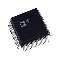
ADSP-2101BS-100 Analog Devices Inc, ADSP-2101BS-100 Datasheet - Page 23

ADSP-2101BS-100
Manufacturer Part Number
ADSP-2101BS-100
Description
IC DSP CONTROLLER 16BIT 80PQFP
Manufacturer
Analog Devices Inc
Series
ADSP-21xxr
Type
Fixed Pointr
Datasheet
1.ADSP-2115BPZ-100.pdf
(64 pages)
Specifications of ADSP-2101BS-100
Rohs Status
RoHS non-compliant
Interface
Synchronous Serial Port (SSP)
Clock Rate
25MHz
Non-volatile Memory
External
On-chip Ram
6kB
Voltage - I/o
5.00V
Voltage - Core
5.00V
Operating Temperature
-40°C ~ 85°C
Mounting Type
Surface Mount
Package / Case
80-MQFP, 80-PQFP
Device Core Size
16b
Architecture
Enhanced Harvard
Format
Fixed Point
Clock Freq (max)
25MHz
Mips
25
Device Input Clock Speed
25MHz
Ram Size
3KB
Program Memory Size
Not RequiredKB
Operating Supply Voltage (typ)
5V
Operating Supply Voltage (min)
4.5V
Operating Supply Voltage (max)
5.5V
Operating Temp Range
-40C to 85C
Operating Temperature Classification
Industrial
Mounting
Surface Mount
Pin Count
80
Package Type
PQFP
Lead Free Status / Rohs Status
Not Compliant
Available stocks
Company
Part Number
Manufacturer
Quantity
Price
REV. B
SPECIFICATIONS (ADSP-2111)
POWER DISSIPATION EXAMPLE
To determine total power dissipation in a specific application,
the following equation should be applied for each output:
C = load capacitance, f = output switching frequency.
Example:
In an ADSP-2111 application where external data memory is
used and no other outputs are active, power dissipation is
calculated as follows:
Assumptions:
•
•
•
•
P
(C
Output
Address, DMS 8
Data, WR
RD
CLKOUT
Total power dissipation for this example = P
ENVIRONMENTAL CONDITIONS
Ambient Temperature Rating:
Package
PGA
PQFP
INT
External data memory is accessed every cycle with 50% of the
address pins switching.
External data memory writes occur every other cycle with
50% of the data pins switching.
Each address and data pin has a 10 pF total load at the pin.
The application operates at V
T
T
PD = Power Dissipation in W
CA
JA
JC
AMB
CASE
= internal power dissipation (from Figure 17).
V
= Thermal Resistance (Junction-to-Ambient)
= Thermal Resistance (Junction-to-Case)
DD
= Thermal Resistance (Case-to-Ambient)
Total Power Dissipation = P
= T
= Case Temperature in C
2
CASE
f ) is calculated for each output:
# of
Pins
9
1
1
– (PD
35 C/W
42 C/W
JA
C
10 pF
10 pF
10 pF
10 pF
C
CA
)
V
DD
DD
2
= 5.0 V and t
INT
V
5
5
5
5
2
2
2
2
DD
V
V
V
V
f
+ (C
2
18 C/W
18 C/W
JC
f
20 MHz = 40.0 mW
10 MHz = 22.5 mW
10 MHz = 2.5 mW
20 MHz = 5.0 mW
INT
V
DD
CK
+ 70.0 mW.
2
= 50 ns.
f )
70.0 mW
17 C/W
23 C/W
CA
–23–
CAPACITIVE LOADING
Figures 18 and 19 show capacitive loading characteristics for the
ADSP-2111.
Figure 19. Typical Output Valid Delay or Hold vs. Load
Capacitance, C
Figure 18. Typical Output Rise Time vs. Load Capacitance, C
(at Maximum Ambient Operating Temperature)
NOMINAL
+12
+10
14
12
10
+8
+6
+4
+2
–2
–4
–6
L
8
6
4
2
(at Maximum Ambient Operating Temperature)
25
25
50
50
V
75
75
C
C
DD
V
L
L
DD
– pF
– pF
= 4.5V
100
100
= 4.5V
125
125
ADSP-21xx
150
150
L


