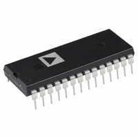
ADMCF326BN Analog Devices Inc, ADMCF326BN Datasheet - Page 8

ADMCF326BN
Manufacturer Part Number
ADMCF326BN
Description
IC DSP FLASH MOTOR CTRLR 28DIP
Manufacturer
Analog Devices Inc
Series
Motor Controlr
Type
Fixed Pointr
Datasheet
1.ADMCF326BN.pdf
(36 pages)
Specifications of ADMCF326BN
Rohs Status
RoHS non-compliant
Interface
Synchronous Serial Port (SSP)
Clock Rate
20MHz
Non-volatile Memory
FLASH (12 kB), ROM (12kB)
On-chip Ram
2.5kB
Voltage - I/o
5.00V
Voltage - Core
5.00V
Operating Temperature
-40°C ~ 85°C
Mounting Type
Through Hole
Package / Case
28-DIP (0.600", 15.24mm)
Lead Free Status / Rohs Status
Not Compliant
ADMCF326
DSP CORE ARCHITECTURE OVERVIEW
Figure 3 is an overall block diagram of the DSP core of the
ADMCF326, which is based on the fixed-point ADSP-2171.
The flexible architecture and comprehensive instruction set of
the ADSP-2171 allow the processor to perform multiple operations
in parallel. In one processor cycle (50 ns with a 10 MHz CLKIN),
the DSP core can:
• Generate the next program address
• Fetch the next instruction
• Perform one or two data moves
• Update one or two data address pointers
• Perform a computational operation
This all takes place while the processor continues to:
• Receive and transmit through the serial port
• Decrement the interval timer
• Generate three-phase PWM waveforms for a power inverter
• Generate two signals using the 8-bit auxiliary PWM timers
• Acquire four analog signals
• Decrement the watchdog timer
The processor contains three independent computational units:
the arithmetic and logic unit (ALU), the multiplier/accumulator
(MAC), and the shifter. The computational units process 16-bit
data directly and have provisions to support multiprecision com-
putations. The ALU performs a standard set of arithmetic and
logic operations as well as provides support for division primitives.
The MAC performs single-cycle multiply, multiply/add, and
multiply/subtract operations with 40 bits of accumulation. The
shifter performs logical and arithmetic shifts, normalization,
denormalization, and derive-exponent operations. The shifter can
be used to efficiently implement numeric format control, including
floating-point representations.
The internal result (R) bus directly connects the computational
units so that the output of any unit may be the input of any unit
on the next cycle.
A powerful program sequencer and two dedicated data address
generators ensure efficient delivery of operands to these compu-
tational units. The sequencer supports conditional jumps and
subroutine calls and returns in a single cycle. With internal loop
counters and loop stacks, the ADMCF326 executes looped code
with zero overhead; no explicit jump instructions are required to
maintain the loop.
Two data address generators (DAGs) provide addresses for
simultaneous dual operand fetches from data memory and pro-
gram memory. Each DAG maintains and updates four address
pointers (I registers). Whenever the pointer is used to access data
(indirect addressing), it is post-modified by the value in one of
four modify (M registers). A length value may be associated with
each pointer (L registers) to implement automatic modulo
addressing for circular buffers. The circular buffering feature is
also used by the serial ports for automatic data transfers to and
from on-chip memory. DAG1 generates only data memory
addresses and provides an optional bit-reversal capability. DAG2
may generate either program or data memory addresses but has
no bit-reversal capability.
–8–
Efficient data transfer is achieved with the use of five
internal buses:
• Program Memory Address (PMA) Bus
• Program Memory Data (PMD) Bus
• Data Memory Address (DMA) Bus
• Data Memory Data (DMD) Bus
• Result (R) Bus
Program Memory on the ADMCF326 can either be internal
(on-chip RAM) or external (Flash). Internal program memory
can store both instructions and data, permitting the ADMCF326
to fetch two operands in a single instruction cycle—one from
program memory and one from data memory. Operation from
external program memory is described in detail in the ADSP-
2100 Family User’s Manual, Third Edition.
The ADMCF326 writes data from its 16-bit registers to the 24-bit
program memory using the PX Register to provide the lower
eight bits. When it reads data (not instructions) from 24-bit pro-
gram memory to a 16-bit data register, the lower eight bits are
placed in the PX Register.
The ADMCF326 can respond to a number of distinct DSP
core and peripheral interrupts. The DSP interrupts comprise
a serial port receive interrupt, a serial port transmit interrupt,
a timer interrupt, and two software interrupts. Additionally,
the motor control peripherals include two PWM interrupts
and a PIO interrupt.
The serial port (SPORT1) provides a complete synchronous
serial interface with optional companding in hardware, and a
wide variety of framed and unframed data transmit and receive
modes of operation. SPORT1 can generate an internal program-
mable serial clock or accept an external serial clock.
A programmable interval counter is also included in the DSP
core and can be used to generate periodic interrupts. A 16-bit
count register (TCOUNT) is decremented every n processor
cycles, where n–1 is a scaling value stored in the 8-bit TSCALE
register. When the value of the counter reaches zero, an interrupt
is generated, and the count register is reloaded from a 16-bit
period register (TPERIOD).
The ADMCF326 instruction set provides flexible data moves
and multifunction instructions (one or two data moves within a
computation) that will execute from internal program memory
RAM. The ADMCF326 assembly language uses an algebraic
syntax for ease of coding and readability. A comprehensive set of
development tools supports program development. For further
information on the DSP core, refer to the ADSP-2100 Family
User’s Manual, Third Edition, with particular reference to
the ADSP-2171.
REV. B


