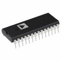
ADMCF326BN Analog Devices Inc, ADMCF326BN Datasheet - Page 12

ADMCF326BN
Manufacturer Part Number
ADMCF326BN
Description
IC DSP FLASH MOTOR CTRLR 28DIP
Manufacturer
Analog Devices Inc
Series
Motor Controlr
Type
Fixed Pointr
Datasheet
1.ADMCF326BN.pdf
(36 pages)
Specifications of ADMCF326BN
Rohs Status
RoHS non-compliant
Interface
Synchronous Serial Port (SSP)
Clock Rate
20MHz
Non-volatile Memory
FLASH (12 kB), ROM (12kB)
On-chip Ram
2.5kB
Voltage - I/o
5.00V
Voltage - Core
5.00V
Operating Temperature
-40°C ~ 85°C
Mounting Type
Through Hole
Package / Case
28-DIP (0.600", 15.24mm)
Lead Free Status / Rohs Status
Not Compliant
ADMCF326
A functional block diagram of the PWM controller is shown in
Figure 6. The generation of the six output PWM signals on pins
AH to CL is controlled by four important blocks:
• The three-phase PWM timing unit, which is the core of the
• The output control unit allows the redirection of the outputs
• The GATE drive unit provides the high chopping frequency
• The PWM shutdown controller manages the two PWM shut-
• The PWM controller is driven by a clock at the same frequency
PWM controller, generates three pairs of complemented and
dead-time-adjusted center-based PWM signals.
of the three-phase timing unit for each channel to either the
high side or low side output. In addition, the output control
unit allows individual enabling/disabling of each of the six
PWM output signals.
and its subsequent mixing with the PWM signals.
down modes (via the PWMTRIP pin, and the PWMSWT
Register) and generates the correct RESET signal for the
Timing Unit.
as the DSP instruction rate, CLKOUT, and is capable of
generating two interrupts to the DSP core. One interrupt is
generated on the occurrence of a PWMSYNC pulse, and
the other is generated on the occurrence of any PWM shut-
down action.
PWM CONFIGURATION
PWMTM (15...0)
PWMDT (9...0)
PWMPD (15...0)
PWMSYNCWT (7...0)
MODECTRL (6)
TO INTERRUPT
CONTROLLER
REGISTERS
PWMSYNC
PWMTRIP
CLK
THREE-PHASE
PWM TIMING
SYNC
UNIT
Figure 6. Overview of the PWM Controller of the ADMCF326
PWM DUTY CYCLE
PWMCHA (15...0)
PWMCHB (15...0)
PWMCHC (15...0)
RESET
REGISTERS
PWM SHUTDOWN CONTROLLER
–12–
Three-Phase Timing Unit
The 16-bit three-phase timing unit is the core of the PWM con-
troller and produces three pairs of pulsewidth modulated signals
with high resolution and minimal processor overhead. There are
four main configuration registers (PWMTM, PWMDT, PWMPD,
and PWMSYNCWT) that determine the fundamental charac-
teristics of the PWM outputs. In addition, the operating mode
of the PWM (Single or Double Update Mode) is selected by Bit 6
of the MODECTRL Register. These registers, in conjunction with
the three 16-bit duty cycle registers (PWMCHA, PWMCHB, and
PWMCHC), control the output of the three-phase timing unit.
PWM Switching Frequency: PWMTM Register
The PWM switching frequency is controlled by the PWM
period register, PWMTM. The fundamental timing unit of
the PWM controller is t
CLKOUT frequency (DSP instruction rate). Therefore, for a
20 MHz CLKOUT, the fundamental time increment is 50 ns.
The value written to the PWMTM Register is effectively the
number of t
required PWMTM value is a function of the desired PWM
switching frequency (f
Therefore, the PWM switching period, T
OR
PWMSEG (8...0)
CONTROL
OUTPUT
SYNC
UNIT
PWMSWT (0)
CK
clock increments in half a PWM period. The
PWMTM
T
S
PWMGATE (9...0)
PWM
=
DRIVE
CK
2
GATE
UNIT
CLK
) and is given by:
×
=
= 1/f
PWMTM
2
f
CLKOUT
×
CLKOUT,
f
PWM
CLKOUT
=
×
S
where f
, can be written as:
t
f
AH
AL
BL
CL
CK
BH
CH
PWMTRIP
f
CLKIN
PWM
CLKOUT,
REV. B
is the


