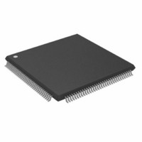
ADSP-2196MKSTZ-160 Analog Devices Inc, ADSP-2196MKSTZ-160 Datasheet - Page 54

ADSP-2196MKSTZ-160
Manufacturer Part Number
ADSP-2196MKSTZ-160
Description
IC DSP CONTROLLER 16BIT 144-LQFP
Manufacturer
Analog Devices Inc
Series
ADSP-21xxr
Type
Fixed Pointr
Datasheet
1.ADSP-2196MKSTZ-160.pdf
(68 pages)
Specifications of ADSP-2196MKSTZ-160
Interface
Host Interface, SPI, SSP, UART
Clock Rate
160MHz
Non-volatile Memory
ROM (48 kB)
On-chip Ram
40kB
Voltage - I/o
3.30V
Voltage - Core
2.50V
Operating Temperature
0°C ~ 70°C
Mounting Type
Surface Mount
Package / Case
144-LQFP
Device Core Size
16b
Format
Fixed Point
Clock Freq (max)
160MHz
Mips
160
Device Input Clock Speed
160MHz
Ram Size
40KB
Program Memory Size
48KB
Operating Supply Voltage (typ)
2.5/3.3V
Operating Supply Voltage (min)
2.37V
Operating Supply Voltage (max)
2.63/3.6V
Operating Temp Range
0C to 70C
Operating Temperature Classification
Commercial
Mounting
Surface Mount
Pin Count
144
Package Type
LQFP
Lead Free Status / RoHS Status
Lead free / RoHS Compliant
Available stocks
Company
Part Number
Manufacturer
Quantity
Price
Company:
Part Number:
ADSP-2196MKSTZ-160
Manufacturer:
Analog Devices Inc
Quantity:
10 000
The P
can drive as shown in
Table 24. P
A typical power consumption can now be calculated for
these conditions by adding a typical internal power dissipa-
tion with the formula in
Figure 30. P
Where:
• P
• P
Note that the conditions causing a worst-case P
different from those causing a worst-case P
P
switching from all ones to all zeros. Note also that it is not
common for an application to have 100% or even 50% of
the outputs switching simultaneously.
Test Conditions
The DSP is tested for output enable, disable, and hold time.
Output Disable Time
Output pins are considered to be disabled when they stop
driving, go into a high impedance state, and start to decay
from their output high or low voltage. The time for the
voltage on the bus to decay by – V is dependent on the
capacitive load, C
can be approximated by the equation in
Figure 31. Decay Time Calculation
REV. PrA
Pin Type
Address
MSx
WR
Data
CLKOUT
September 2001
INT
Power Dissipation on page 52
EXT
INT
cannot occur while 100% of the output pins are
EXT
is I
is from
DDINT
equation is calculated for each class of pins that
EXT
TOTAL
# of Pins
15
1
1
16
1
Table 24
Calculation
This information applies to a product under development. Its characteristics and specifications are subject to change with-
out notice. Analog Devices assumes no obligation regarding future manufacturing unless otherwise agreed to in writing.
2.5V, using the calculation I
L
P
(Typical) Calculation
and the load current, I
TOTAL
t
DECAY
Table
Figure
=
P
24.
=
EXT
% Switching
50
0
—
50
—
For current information contact Analog Devices at 800/262-5643
30.
C
---------------
L
I
+
L
P
V
INT
Figure
L
. This decay time
INT
DDINT
. Maximum
31.
EXT
TBD pF
TBD pF
TBD pF
TBD pF
TBD pF
listed in
are
C
The output disable time t
t
t
switches to when the output voltage decays –V from the
measured output high or output low voltage. The t
calculated with test loads C
0.5 V.
Figure 32. Output Enable/Disable
Output Enable Time
Output pins are considered to be enabled when they have
made a transition from a high impedance state to when they
start driving. The output enable time t
from when a reference signal reaches a high or low voltage
level to when the output has reached a specified high or low
trip point, as shown in the Output Enable/Disable diagram
(Figure
enabled, the measurement value is that of the first pin to
start driving.
MEASURED
MEASURED
25.0 MHz
25.0 MHz
25 MHz
25.0 MHz
100 MHz
f
32). If multiple pins (such as the data bus) are
and t
is the interval from when the reference signal
DECAY
as shown in
10.9 V
10.9 V
10.9 V
10.9 V
V
10.9 V
DIS
DD
L
is the difference between
2
and I
Figure
L
, and with –V equal to
= P
=TBD W
=TBD W
=TBD W
=TBD W
=TBD W
P
ENA
EXT
32. The time
ADSP-2196
EXT
=TBD W
is the interval
DECAY
54
is


