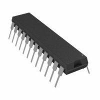
AD7237KN Analog Devices Inc, AD7237KN Datasheet - Page 9

AD7237KN
Manufacturer Part Number
AD7237KN
Description
IC DAC 12BIT LC2MOS DUAL 24-DIP
Manufacturer
Analog Devices Inc
Series
DACPORT®r
Specifications of AD7237KN
Data Interface
Parallel
Rohs Status
RoHS non-compliant
Settling Time
8µs
Number Of Bits
12
Number Of Converters
2
Voltage Supply Source
Dual ±
Operating Temperature
-40°C ~ 85°C
Mounting Type
Through Hole
Package / Case
24-DIP (0.300", 7.62mm)
Resolution (bits)
12bit
Sampling Rate
125kSPS
Input Channel Type
Parallel
Supply Current
11mA
Digital Ic Case Style
DIP
No. Of Pins
24
Current, Supply
± 10 μA (Max.)
Differential Nonlinearity
± 0.9 LSB (Min.)
Offset Error
± 3 LBS (Max.)
Package Type
PDIP
Power Dissipation
1000 mW
Resolution
12 Bits
Temperature, Operating, Maximum
85 °C
Temperature, Operating, Minimum
-40 °C
Voltage, Input Range
5.25 V (Max.) (Ref.)
Voltage, Supply
2.4 V (Min.)
Power Dissipation (max)
-
Lead Free Status / RoHS Status
Contains lead / RoHS non-compliant
REV. 0
CSA
X
1
0
1
0
X = Don’t Care
INTERFACE LOGIC INFORMATION—AD7237A
The input loading structure on the AD7237A is configured for
interfacing to microprocessors with an 8-bit-wide data bus. The
part contains two 12-bit latches per DAC—an input latch and a
DAC latch. Each input latch is further subdivided into a least
significant 8-bit latch and a most significant 4-bit latch. Only
the data held in the DAC latches determines the outputs from
the part. The input control logic for the AD7237A is shown in
Figure 6, while the write cycle timing diagram is shown in
Figure 7.
CS, WR, A0 and A1 control the loading of data to the input
latches. The eight data inputs accept right-justified data. Data
can be loaded to the input latches in any sequence. Provided
that LDAC is held high, there is no analog output change as a
result of loading data to the input latches. Address lines A0 and
A1 determine which latch data is loaded to when CS and WR
are low. The selection of the input latches is shown in the truth
table for AD7237A operation in Table II.
The LDAC input controls the transfer of 12-bit data from the
input latches to the DAC latches. Both DAC latches, and hence
both analog outputs, are updated at the same time. The LDAC
signal is level triggered, and data is latched into the DAC latch
on the rising edge of LDAC. The LDAC input is asynchronous
and independent of WR. This is useful in many applications
especially in the simultaneous updating of multiple AD7237As.
CSB
X
1
1
0
0
Table I. AD7247A Truth Table
WR
1
X
0
0
0
Function
No Data Transfer
No Data Transfer
DAC A Latch Transparent
DAC B Latch Transparent
Both DAC Latches Transparent
Figure 6. AD7237A Input Control Logic
–9–
CS WR A1 A0 LDAC Function
1
X
0
0
0
0
1
X = Don’t Care.
However, care must be taken while exercising LDAC during a
write cycle. If an LDAC operation overlaps a CS and WR op-
eration, there is a possibility of invalid data being latched to the
output. To avoid this, LDAC must remain low after CS or WR
return high for a period equal to or greater than t
mum LDAC pulse width.
X
1
0
0
0
0
1
Figure 7. AD7237A Write Cycle Timing Diagram
X X 1
X X 1
0
0
1
1
X X 0
0
1
0
1
Table II. AD7237A Truth Table
1
1
1
1
No Data Transfer
No Data Transfer
DAC A LS Input Latch Transparent
DAC A MS Input Latch Transparent
DAC B LS Input Latch Transparent
DAC B MS Input Latch Transparent
DAC A and DAC B DAC Latches
Updated Simultaneously from the
Respective Input Latches
AD7237A/AD7247A
8
, the mini-


