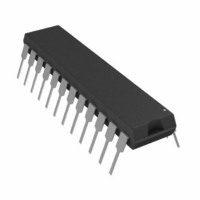
AD7237KN Analog Devices Inc, AD7237KN Datasheet - Page 4

AD7237KN
Manufacturer Part Number
AD7237KN
Description
IC DAC 12BIT LC2MOS DUAL 24-DIP
Manufacturer
Analog Devices Inc
Series
DACPORT®r
Specifications of AD7237KN
Data Interface
Parallel
Rohs Status
RoHS non-compliant
Settling Time
8µs
Number Of Bits
12
Number Of Converters
2
Voltage Supply Source
Dual ±
Operating Temperature
-40°C ~ 85°C
Mounting Type
Through Hole
Package / Case
24-DIP (0.300", 7.62mm)
Resolution (bits)
12bit
Sampling Rate
125kSPS
Input Channel Type
Parallel
Supply Current
11mA
Digital Ic Case Style
DIP
No. Of Pins
24
Current, Supply
± 10 μA (Max.)
Differential Nonlinearity
± 0.9 LSB (Min.)
Offset Error
± 3 LBS (Max.)
Package Type
PDIP
Power Dissipation
1000 mW
Resolution
12 Bits
Temperature, Operating, Maximum
85 °C
Temperature, Operating, Minimum
-40 °C
Voltage, Input Range
5.25 V (Max.) (Ref.)
Voltage, Supply
2.4 V (Min.)
Power Dissipation (max)
-
Lead Free Status / RoHS Status
Contains lead / RoHS non-compliant
AD7237A/AD7247A
Pin
1
2
3
4
5
6
7
8-10
11
12
13
14
15
16
17
18
19
20
21
22
23
24
Mnemonic
REF INA
REF OUT
REF INB
R
V
AGND
DB7
DB6-DB4
DB3
DGND
DB2
DB1
DB0
A0
A1
CS
WR
LDAC
V
V
V
R
OUTB
DD
OUTA
SS
OFSA
OFSB
Description
Voltage Reference Input for DAC A. The reference voltage for DAC A is applied to this pin. It is internally
buffered before being applied to the DAC. The nominal reference voltage for correct operation of the
AD7237A is 5 V.
Voltage Reference Output. The internal 5 V analog reference is provided at this pin. To operate the part with
internal reference, REF OUT should be connected to REF INA, REF INB.
Voltage Reference Input for DAC B. The reference voltage for DAC B is applied to this pin. It is internally
buffered before being applied to the DAC. The nominal reference voltage for correct operation of the
AD7237A is 5 V.
Output Offset Resistor for DAC B. This input configures the output ranges for DAC B. It is connected to
V
Analog Output Voltage from DAC B. This is the buffer amplifier output voltage. Three different output
voltage ranges can be chosen: 0 V to +5 V, 0 V to +10 V and 5 V. The amplifier is capable of developing
+10 V across a 2 k resistor to GND.
Analog Ground. Ground reference for DACs, reference and output buffer amplifiers.
Data Bit 7.
Data Bit 6 to Data Bit 4.
Data Bit 3/Data Bit 11 (MSB).
Digital Ground. Ground reference for digital circuitry.
Data Bit 2/Data Bit 10.
Data Bit 1/Data Bit 9.
Data Bit 0 (LSB)/Data Bit 8.
Address Input. Least significant address input for input latches. A0 and A1 select which of the four input
latches data is written to (see Table II).
Address Input. Most significant address input for input latches.
Chip Select. Active low logic input. The device is selected when this input is active.
Write Input. WR is an active low logic input which is used in conjunction with CS, A0 and A1 to write data
to the input latches.
Load DAC. Logic input. A new word is loaded into the DAC latches from the respective input latches on the
falling edge of this signal.
Positive Supply (+12 V to +15 V).
Analog Output Voltage from DAC A. This is the buffer amplifier output voltage. Three different output
voltage ranges can be chosen: 0 V to +5 V, 0 V to +10 V and 5 V. The amplifier is capable of developing
+10 V across a 2 k resistor to GND.
Negative Supply (0 V or –12 V to –15 V).
Output Offset Resistor for DAC A. This input configures the output ranges for DAC A. It is connected to
V
OUTB
OUTA
for the +5 V range, to AGND for the +10 V range and to REF INB for the 5 V range.
for the +5 V range, to AGND for the +10 V range and to REF INA for the 5 V range.
AD7237A PIN FUNCTION DESCRIPTION (DIP PIN NUMBERS)
–4–
REV. 0


