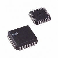
AD7225KP-REEL Analog Devices Inc, AD7225KP-REEL Datasheet - Page 9

AD7225KP-REEL
Manufacturer Part Number
AD7225KP-REEL
Description
IC DAC 8BIT QUAD W/AMP 28-PLCC
Manufacturer
Analog Devices Inc
Datasheet
1.AD7225CRSZ.pdf
(24 pages)
Specifications of AD7225KP-REEL
Rohs Status
RoHS non-compliant
Settling Time
4µs
Number Of Bits
8
Number Of Converters
4
Voltage Supply Source
Dual ±
Power Dissipation (max)
500mW
Operating Temperature
-40°C ~ 85°C
Mounting Type
Surface Mount
Package / Case
28-LCC (J-Lead)
Data Interface
-
Available stocks
Company
Part Number
Manufacturer
Quantity
Price
Company:
Part Number:
AD7225KP-REEL
Manufacturer:
Analog Devices Inc
Quantity:
10 000
CIRCUIT INFORMATION
DIGITAL-TO-ANALOG SECTION
The AD7225 contains four identical, 8-bit voltage mode digital-
to-analog converters. Each DAC has a separate reference input.
The output voltages from the converters have the same polarity
as the reference voltages, allowing single-supply operation. A novel
DAC switch pair arrangement on the AD7225 allows a refer-
ence voltage range from 2 V to 12.5 V on each reference input.
Each DAC consists of a highly stable, thin-film, R-2R ladder and
eight high speed NMOS, single-pole, double-throw switches. The
simplified circuit diagram for Channel A is shown in Figure 10.
Note that AGND is common to all four DACs.
The input impedance at any of the reference inputs is code
dependent and can vary from 11 kΩ minimum to infinity. The
lowest input impedance at any reference input occurs when that
DAC is loaded with Digital Code 01010101. Therefore, it is
important that the reference presents a low output impedance
under changing load conditions. The nodal capacitance at the
reference terminals is also code dependent and typically varies
from 15 pF to 35 pF.
Each V
voltage source with an output voltage of
where D
and can vary from 0 to 255/256.
The output impedance is that of the output buffer amplifier.
OP AMP SECTION
Each voltage mode DAC output is buffered by a unity gain
noninverting CMOS amplifier. This buffer amplifier is capable
of developing 10 V across a 2 kΩ load and can drive capacitive
loads of 3300 pF.
The AD7225 can be operated single or dual supply; operating
with dual supplies results in enhanced performance in some
V
AGND
V
REF
OUTX
OUT
A
X
Figure 10. Digital-to-Analog Simplified Circuit Diagram
is a fractional representation of the digital input code
x pin can be considered a digitally programmable
= D
2R
X
× V
DB0
2R
R
REFX
DB5
2R
R
DB6
2R
R
SHOWN FOR ALL 1s ON DAC
DB7
2R
V
OUT
A
Rev. C | Page 9 of 24
parameters that cannot be achieved with single-supply opera-
tion. In single-supply operation (V
capability of the amplifier, which is normally 400 μA, is reduced
as the output voltage nears AGND. The full sink capability of
400 μA is maintained over the full output voltage range by tying
V
Settling time for negative-going output signals approaching
AGND is similarly affected by V
for single-supply operation is longer than for dual-supply opera-
tion. Positive-going settling time is not affected by V
Additionally, the negative V
output amplifiers, which results in better zero code perfor-
mance and improved slew rate at the output than can be
obtained in the single-supply mode.
DIGITAL INPUTS SECTION
The AD7225 digital inputs are compatible with either TTL or
5 V CMOS levels. All logic inputs are static protected MOS
gates with typical input currents of less than 1 nA. Internal
input protection is achieved by an on-chip distributed diode
between DGND and each MOS gate. To minimize power supply
currents, it is recommended that the digital input voltages be
driven as close to the supply rails (V
cally possible.
SS
to −5 V. This is shown in Figure 11.
500
400
300
200
100
0
0
V
SS
= –5V
Figure 11. Variation of I
V
SS
2
= 0V
SS
4
gives more headroom to the
V
OUT
SS
. Negative-going settling time
SS
(V)
DD
SINK
= 0 V = AGND), the sink
6
and DGND) as practi-
with V
OUT
8
V
T
A
DD
= 25°C
AD7225
= +15V
SS
.
10


