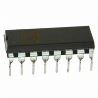
AD7249BN Analog Devices Inc, AD7249BN Datasheet - Page 4

AD7249BN
Manufacturer Part Number
AD7249BN
Description
IC DAC 12BIT SRL W/REF 16-DIP
Manufacturer
Analog Devices Inc
Series
DACPORT®r
Datasheet
1.AD7249ARZ.pdf
(12 pages)
Specifications of AD7249BN
Rohs Status
RoHS non-compliant
Settling Time
10µs
Number Of Bits
12
Data Interface
Serial
Number Of Converters
2
Voltage Supply Source
Dual ±
Power Dissipation (max)
300mW
Operating Temperature
-40°C ~ 85°C
Mounting Type
Through Hole
Package / Case
16-DIP (0.300", 7.62mm)
AD7249
Pin
11
12
13
14
15
16
17
18
19
10
11
12
13
14
15
16
Mnemonic
REFOUT
REFIN
R
V
AGND
CLR
BIN/COMP
DGND
SDIN
LDAC
SCLK
SYNC
V
V
V
R
OFSB
OUTB
DD
OUTA
SS
OFSA
BIN/COMP
REFOUT
PIN CONFIGURATIONS
REFIN
R
V
AGND
DGND
OUTB
OFSB
CLR
(DIP and SOIC)
1
2
3
4
5
6
7
8
(Not to Scale)
TOP VIEW
AD7249
Description
Voltage Reference Output. The internal 5 V analog reference is provided at this pin. To operate the
part using its internal reference, REFOUT should be connected to REFIN.
Voltage Reference Input. It is internally buffered before being applied to both DACs. The nominal
reference voltage for specified operation of the AD7249 is 5 V.
Output Offset Resistor for the amplifier of DAC B. It is connected to V
AGND for the +10 V range and to REFIN for the –5 V to +5 V range.
Analog Output Voltage of DAC B. This is the buffer amplifier output voltage. Three different output
voltage ranges can be chosen: 0 V to +5 V, 0 V to +10 V and –5 V to +5 V.
Analog Ground. Ground reference for all analog circuitry.
Clear, Logic Input. Taking this input low clears both DACs. It sets V
unipolar ranges and the twos complement bipolar range and to –REFIN in the offset binary bipolar
range.
Logic Input. This input selects the data format to be either binary or twos complement. In both uni-
polar ranges natural binary format is selected by connecting this input to a Logic “0”. In the bipolar
configuration offset binary format is selected with a Logic “0” while a Logic “1” selects twos complement.
Digital Ground. Ground reference for all digital circuitry.
Serial Data In, Logic Input. The 16-bit serial data word is applied to this input.
Load DAC, Logic Input. Updates both DAC outputs. The DAC outputs are updated on the falling
edge of this signal or alternatively if this line is permanently low, an automatic update mode is se-
lected whereby both DACs are updated on the 16th falling SCLK pulse.
Serial Clock, Logic Input. Data is clocked into the input register on each falling SCLK edge.
Data Synchronization Pulse, Logic Input. Taking this input low initializes the internal logic in readi-
ness for a new data word.
Positive Power Supply.
Analog Output Voltage of DAC A. This is the buffer amplifier output voltage. Three different output
voltage ranges can be chosen: 0 V to +5 V, 0 V to +10 V and –5 V to +5 V.
Negative Power Supply (used for the output amplifier only) may be connected to 0 V for single sup-
ply operation or –12 V to –15 V for dual supplies.
Output Offset Resistor for the amplifier of DAC A. It is connected to V
AGND for the +10 V range and to REFIN for the –5 V to +5 V range.
PIN FUNCTION DESCRIPTION (DIP & SOIC PIN NUMBERS)
16
15
14
13
12
11
10
9
R
V
V
V
SYNC
SCLK
LDAC
SDIN
SS
OUTA
DD
OFSA
Model
AD7249AN
AD7249BN
AD7249AR
AD7249BR
AD7249SQ
NOTE
1
Available to /883B processing only. Contact your local sales office for military
data sheet.
1
–40°C to +85°C
–40°C to +85°C
–40°C to +85°C
–40°C to +85°C
–55°C to +125°C
Temperature
Range
ORDERING GUIDE
OUTA
OUTB
OUTA
and V
Relative
Accuracy
± 1 LSB
± 1/2 LSB
± 1 LSB
± 1/2 LSB
± 1 LSB
for the +5 V range, to
for the +5 V range, to
OUTB
to 0 V in both
Package
Option
N-16
N-16
R-16
R-16
Q-16


