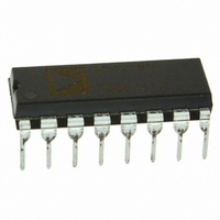
AD7249BN Analog Devices Inc, AD7249BN Datasheet - Page 11

AD7249BN
Manufacturer Part Number
AD7249BN
Description
IC DAC 12BIT SRL W/REF 16-DIP
Manufacturer
Analog Devices Inc
Series
DACPORT®r
Datasheet
1.AD7249ARZ.pdf
(12 pages)
Specifications of AD7249BN
Rohs Status
RoHS non-compliant
Settling Time
10µs
Number Of Bits
12
Data Interface
Serial
Number Of Converters
2
Voltage Supply Source
Dual ±
Power Dissipation (max)
300mW
Operating Temperature
-40°C ~ 85°C
Mounting Type
Through Hole
Package / Case
16-DIP (0.300", 7.62mm)
AD7249–68HC11 Interface
Figure 14 shows a serial interface between the AD7249 and the
68HC11 microcontroller. SCK of the 68HC11 drives SCLK of
the AD7249 while the MOSI output drives the serial data line
of the AD7249. The SYNC signal is derived from a port line
(PC0 shown).
For correct operation of this interface, the 68HC11 should be
configured such that its CPOL bit is a 0 and its CPHA bit is a
1. When data is to be transmitted to the part, PC0 is taken low.
When the 68HC11 is configured like this, data on MOSI is
valid on the falling edge of SCK. The 68HC11 transmits its
serial data in 8-bit bytes with only eight falling clock edges
occurring in the transmit cycle. To load data to the AD7249,
PC0 is left low after the first eight bits are transferred and a sec-
ond byte of data is then transferred serially to the AD7249.
When the second serial transfer is complete, the PC0 line is
taken high.
Figure 14 shows the LDAC input of the AD7249 being driven
from another bit programmable port line (PC1). As a result,
both DACs can be updated simultaneously by taking LDAC
low after both DACs latches have updated.
AD7249–87C51 Interface
A serial interface between the AD7249 and the 87C51 micro-
controller is shown in Figure 15. TXD of the 87C51 drives
SCLK of the AD7249 while RXD drives the serial data line of
the part. The SYNC signal is derived from the port line P3.3
and the LDAC line is driven port line P3.2.
The 87C51 provides the LSB of its SBUF register as the first
bit in the serial data stream. Therefore, the user will have to
ensure that the data in the SBUF register is arranged correctly
so that the don’t care bits are the first to be transmitted to the
AD7249 and the last bit to be sent is the LSB of the word to be
loaded to the AD7249. When data is to be transmitted to the
part, P3.3 is taken low. Data on RXD is valid on the falling
edge of TXD. The 87C51 transmits its serial data in 8-bit bytes
with only eight falling clock edges occurring in the transmit
cycle. To load data to the AD7249, P3.3 is left low after the
first eight bits are transferred, and a second byte of data is then
transferred serially to the AD7249 with DB12 used to select
the appropriate DAC register. When the second serial transfer
is complete, the P3.3 line is taken high and then taken low
again to start the loading sequence to the second DAC (see
timing diagram Figure 8).
*ADDITIONAL PINS OMITTED FOR CLARITY.
68HC11*
MOSI
SCK
PC1
PC0
LDAC
SCLK
SYNC
SDIN
AD7249*
Figure 15 shows the LDAC input of the AD7249 driven from
the bit programmable port line P3.2. As a result, both DAC
outputs can be updated simultaneously by taking the LDAC
line low following the completion of the write cycle to the sec-
ond DAC. Alternatively LDAC could be hardwired low and the
analog output will be updated on the sixteenth falling edge of
TXD after the SYNC signal for the DAC has gone low.
APPLICATIONS
OPTO-ISOLATED INTERFACE
In many process control type applications it is necessary to
provide an isolation barrier between the controller and the
unit being controlled. Opto-isolators can provide voltage
isolation in excess of 3 kΩ. The serial loading structure of the
AD7249 makes it ideal for opto-isolated interfaces as the num-
ber of interface lines is kept to a minimum.
Figure 16 shows a 2-channel isolated interface using the
AD7249.
The sequence of events to program the output channels is as
follows.
1. Take the SYNC line low.
2. Transmit the 16-bit word for DAC A (DB 12 of the 16-bit
3. Bring SYNC line low again and transmit 16 bits for DAC B,
4. Pulse the LDAC line low. This updates both output chan-
data word selects the DAC, DB12 = 0 to select DAC A) and
bring the SYNC line high after the 16 bits have been trans-
mitted.
bring SYNC back high at end of transmission.
nels simultaneously on the falling edge of LDAC.
*ADDITIONAL PINS OMITTED FOR CLARITY.
87C51*
RXD
P3.2
P3.3
TXD
LDAC
SYNC
SCLK
SDIN
AD7249*
AD7249


