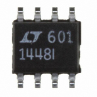
LTC1448IS8#TRPBF Linear Technology, LTC1448IS8#TRPBF Datasheet - Page 6

LTC1448IS8#TRPBF
Manufacturer Part Number
LTC1448IS8#TRPBF
Description
IC D/A CONV 12BIT R-R DUAL 8SOIC
Manufacturer
Linear Technology
Datasheet
1.LTC1448CN8PBF.pdf
(12 pages)
Specifications of LTC1448IS8#TRPBF
Settling Time
14µs
Number Of Bits
12
Data Interface
Serial
Number Of Converters
2
Voltage Supply Source
Single Supply
Power Dissipation (max)
2.5mW
Operating Temperature
-40°C ~ 85°C
Mounting Type
Surface Mount
Package / Case
8-SOIC (3.9mm Width)
Lead Free Status / RoHS Status
Lead free / RoHS Compliant
Available stocks
Company
Part Number
Manufacturer
Quantity
Price
OPERATIO
DEFI ITIO S
LTC1448
Differential Nonlinearity (DNL): The differerence
between the measured change and the ideal 1LSB change
for any two adjacent codes. The DNL error between any
two codes is calculated as follows:
where V
two adjacent codes.
Digital Feedthrough: The glitch that appears at the analog
output caused by AC coupling from the digital inputs when
they change state. The area of the glitch is specified in
(nV)(sec).
Full-Scale Error (FSE): The deviation of the actual full-
scale voltage from ideal. FSE includes the effects of offset
and gain errors (see Applications Information).
Integral Nonlinearity (INL): The deviation from a straight
line passing through the endpoints of the DAC transfer
curve (Endpoint INL). Because the output cannot go below
zero, the linearity is measured between full scale and the
lowest code which guarantees the output will be greater
Serial Interface
The data on the DIN input is loaded into the shift register
on the rising edge of the clock. Data is loaded as one 24-
bit word where the first 12 bits are for DAC A and the
second 12 are for DAC B. For each 12-bit segment the MSB
is loaded first. Data from the shift register is loaded into the
DAC register when CS/LD is pulled high. The clock is
disabled internally when CS/LD is high. Note: CLK must be
low before CS/LD is pulled low to avoid an extra internal
clock pulse.
Voltage Output
The LTC1448’s rail-to-rail buffered outputs can source or
sink 5mA over the entire operating temperature range
6
DNL = ( V
U
OUT
OUT
is the measured voltage difference between
U
U
– LSB)/LSB
than zero. The INL error at a given input code is calculated
as follows:
where V
the given input code.
Least Significant Bit (LSB): The ideal voltage difference
between two successive codes.
Resolution (n): Defines the number of DAC output states
(2
imply linearity.
Voltage Offset Error (V
output when the DAC is loaded with all zeros. A single
supply DAC can have a true negative offset, but the output
cannot go below zero (see Applications Information).
For this reason, single supply DAC offset is measured at
the lowest code that guarantees the output will be greater
than zero.
while pulling to within 300mV of the positive supply
voltage or ground. The output swings to within a few
millivolts of either supply rail when unloaded and has an
equivalent output resistance of 30 when driving a load to
the rails. The output can drive 1000pF without going into
oscillation.
The output swings from 0V to the voltage at the REF pin,
i.e., there is a gain of 1 from the REF to V
if REF is tied to V
(V
n
CC
INL = [V
LSB = V
) that divide the full-scale range. Resolution does not
– V
OUT
OS
REF
). See Applications Information.
OUT
is the output voltage of the DAC measured at
/4096
– V
OS
CC
– (V
OS
the output can only swing to
FS
): Nominally, the voltage at the
– V
OS
)(code/4095)]/LSB
OUT
. Please note


