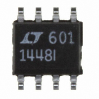
LTC1448IS8#TRPBF Linear Technology, LTC1448IS8#TRPBF Datasheet - Page 3

LTC1448IS8#TRPBF
Manufacturer Part Number
LTC1448IS8#TRPBF
Description
IC D/A CONV 12BIT R-R DUAL 8SOIC
Manufacturer
Linear Technology
Datasheet
1.LTC1448CN8PBF.pdf
(12 pages)
Specifications of LTC1448IS8#TRPBF
Settling Time
14µs
Number Of Bits
12
Data Interface
Serial
Number Of Converters
2
Voltage Supply Source
Single Supply
Power Dissipation (max)
2.5mW
Operating Temperature
-40°C ~ 85°C
Mounting Type
Surface Mount
Package / Case
8-SOIC (3.9mm Width)
Lead Free Status / RoHS Status
Lead free / RoHS Compliant
Available stocks
Company
Part Number
Manufacturer
Quantity
Price
ELECTRICAL CHARACTERISTICS
SYMBOL
AC Performance
Reference Input
R
REF
Digital I/O
V
V
I
C
Switching (V
t
t
t
t
t
t
t
t
t
t
t
t
t
t
t
t
The
temperature range.
Note 1: Nonlinearity is defined from code 20 to code 4095 (full scale).
See Applications Information.
Note 2: Load is 5k in parallel with 100pF.
Note 3: DAC switched between all 1s and the code corresponding to V
for the part.
V
LEAK
1
2
3
4
5
6
7
8
Switching (V
1
2
3
4
5
6
7
8
IH
IL
IN
CC
IN
= 2.7V to 5.5V, V
denotes specifications which apply over the full operating
PARAMETER
Voltage Output Slew Rate
Voltage Output Settling Time
Digital Feedthrough
REF Input Resistance
REF Input Range
Digital Input High Voltage
Digital Input Low Voltage
Digital Input Leakage
Digital Input Capacitance
D
D
CLK High Time
CLK Low Time
CS/LD Pulse Width
LSB CLK to CS/LD
CS/LD Low to CLK
CLK Low to CS/LD Low
D
D
CLK High Time
CLK Low Time
CS/LD Pulse Width
LSB CLK to CS/LD
CS/LD Low to CLK
CLK Low to CS/LD Low
CC
CC
IN
IN
IN
IN
= 4.5V to 5.5V)
Valid to CLK Setup
Valid to CLK Hold
= 2.7V to 5.5V)
Valid to CLK Setup
Valid to CLK Hold
OUT A
and V
OUT B
unloaded, REF V
(Notes 2, 3) to ± 0.5LSB
CONDITIONS
(Notes 5, 6)
V
V
V
V
V
(Note 6)
(Note 6)
(Note 6)
(Note 6)
(Note 6)
(Note 6)
(Note 6)
(Note 6)
(Note 6)
(Note 6)
(Note 6)
(Note 6)
(Note 6)
CC
CC
CC
CC
IN
= GND to V
= 5V
= 3V
= 5V
= 3V
CC
CC
, T
OS
A
= T
MIN
Note 4: Digital inputs at 0V or V
Note 5: V
output is unloaded.
Note 6. Guaranteed by design, not subject to test.
to T
MAX
, unless otherwise noted.
OUT
can only swing from (GND + V
CC
MIN
0.5
7.5
2.4
2.0
.
40
40
40
50
40
20
20
60
60
60
80
60
30
30
0
0
0
12.5
TYP
1.0
0.3
14
OS
) to (V
MAX
LTC1448
± 10
V
0.8
0.6
18
10
CC
CC
– V
OS
) when
UNITS
nV • s
3
V/µs
k
µA
µs
pF
ns
ns
ns
ns
ns
ns
ns
ns
ns
ns
ns
ns
ns
ns
ns
ns
V
V
V
V
V


