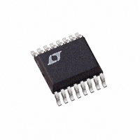
LTC1665IGN Linear Technology, LTC1665IGN Datasheet - Page 4

LTC1665IGN
Manufacturer Part Number
LTC1665IGN
Description
IC D/A CONV 8BIT OCTAL 16-SSOP
Manufacturer
Linear Technology
Datasheet
1.LTC1665CGNPBF.pdf
(16 pages)
Specifications of LTC1665IGN
Settling Time
30µs
Number Of Bits
8
Data Interface
Serial
Number Of Converters
8
Voltage Supply Source
Single Supply
Power Dissipation (max)
1mW
Operating Temperature
-40°C ~ 85°C
Mounting Type
Surface Mount
Package / Case
16-SSOP
Lead Free Status / RoHS Status
Contains lead / RoHS non-compliant
Available stocks
Company
Part Number
Manufacturer
Quantity
Price
Company:
Part Number:
LTC1665IGN
Manufacturer:
LT
Quantity:
10 000
Part Number:
LTC1665IGN
Manufacturer:
LT
Quantity:
20 000
Part Number:
LTC1665IGN#PBF
Manufacturer:
LT/凌特
Quantity:
20 000
LTC1665/LTC1660
range, otherwise specifications are at T
SYMBOL
t
t
t
t
t
t
Note 1: Absolute maximum ratings are those values beyond which the life
of a device may be impaired.
Note 2: Nonlinearity and monotonicity are defined from code 4 to code
255 for the LTC1665 and from code 20 to code 1023 for the LTC1660.
See Applications Information.
Note 3: Digital inputs at 0V or V
Note 4: Load is 10k in parallel with 100pF.
TYPICAL PERFOR A CE CHARACTERISTICS
TI I G CHARACTERISTICS
4
6
7
8
9
10
11
W
U
PARAMETER
LSB SCK High to CS/LD High
CS/LD Low to SCK High
D
SCK Low to CS/LD Low
CLR Pulse Width
CS/LD High to SCK Positive Edge
SCK Frequency
OUT
Propagation Delay
2.9
2.8
2.7
2.6
2.5
2.4
2.3
2.2
2.1
3
2
–30
Midscale Output Voltage
vs Load Current
V
CODE = 128 (LTC1665)
CODE = 512 (LTC1660)
REF
CC
–20
= V
.
CC
W
SOURCE
–10
V
V
V
I
CC
CC
CC
OUT
U
= 5.5V
= 5V
= 4.5V
A
0
(mA)
= 25 C. (See Figure 1)
SINK
10
20
The
1665/60 G01
CONDITIONS
(Note 6)
(Note 6)
C
(Note 6)
(Note 6)
(Note 6)
Continuous Square Wave (Note 6)
Continuous 28% Duty Cycle Pulse
Gated Square Wave
LOAD
30
denotes specifications which apply over the full operating temperature
= 15pF (Note 6)
Note 5: V
i.e., codes 26 and 230 for the LTC1665 or codes 102 and 922 for the
LTC1660.
Note 6: Guaranteed by design and not production tested.
Note 7: Measured at code 4 for the LTC1665 and code 20 for the
LTC1660.
1.9
1.8
1.7
1.6
1.5
1.4
1.3
1.2
1.1
CC
2
1
–15
Midscale Output Voltage
vs Load Current
= V
V
CODE = 128 (LTC1665)
CODE = 512 (LTC1660)
(LTC1665/LTC1660)
REF
–12
REF
= V
= 5V. DAC switched between 0.1V
– 8
CC
V
V
CC
CC
SOURCE
– 4
V
= 3.6V
= 3V
CC
I
OUT
= 2.7V
0
(mA)
MIN
100
120
50
30
30
5
SINK
4
8
1665/60 G02
TYP
12 15
27
47
41
5
0
0
FS
and 0.9V
MAX
3.85
5.55
150
10
FS
,
UNITS
MHz
MHz
MHz
ns
ns
ns
ns
ns
ns


