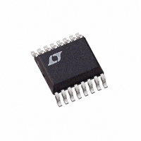
LTC1665IGN Linear Technology, LTC1665IGN Datasheet - Page 10

LTC1665IGN
Manufacturer Part Number
LTC1665IGN
Description
IC D/A CONV 8BIT OCTAL 16-SSOP
Manufacturer
Linear Technology
Datasheet
1.LTC1665CGNPBF.pdf
(16 pages)
Specifications of LTC1665IGN
Settling Time
30µs
Number Of Bits
8
Data Interface
Serial
Number Of Converters
8
Voltage Supply Source
Single Supply
Power Dissipation (max)
1mW
Operating Temperature
-40°C ~ 85°C
Mounting Type
Surface Mount
Package / Case
16-SSOP
Lead Free Status / RoHS Status
Contains lead / RoHS non-compliant
Available stocks
Company
Part Number
Manufacturer
Quantity
Price
Company:
Part Number:
LTC1665IGN
Manufacturer:
LT
Quantity:
10 000
Part Number:
LTC1665IGN
Manufacturer:
LT
Quantity:
20 000
Part Number:
LTC1665IGN#PBF
Manufacturer:
LT/凌特
Quantity:
20 000
OPERATIO
LTC1665/LTC1660
Table 2. DAC Address/Control Functions
state and all DAC settings are retained in memory so that
when Sleep mode is exited, the outputs of DACs not
updated by the Wake command are restored to their last
active state.
Sleep mode is initiated by performing a load sequence to
address 1110
ignored). Once in Sleep mode, a load sequence to any
other address (including “No Change” addresses 0000
and 1001-1101
It is possible to keep one or more chips of a daisy chain in
continuous Sleep mode by giving the Sleep instruction to
these chips each time the active chips in the chain are
updated.
10
A3
0
0
0
0
0
0
0
0
1
1
1
1
1
1
1
1
ADDRESS/CONTROL
A2
0
0
0
0
1
1
1
1
0
0
0
0
1
1
1
1
b
b
(the DAC input word D7-D0 [D9-D0] is
) causes the LTC1665/LTC1660 to Wake.
A1
0
0
1
1
0
0
1
1
0
0
1
1
0
0
1
1
U
A0
0
1
0
1
0
1
0
1
0
1
0
1
0
1
0
1
Load ALL DACs
8/10-Bit Code
DAC STATUS
Load DAC A
Load DAC B
Load DAC C
Load DAC D
Load DAC E
Load DAC G
Load DAC H
Load DAC F
No Change
No Change
No Change
No Change
No Change
No Change
No Change
with Same
SLEEP STATUS
Sleep
Wake
Wake
Wake
Wake
Wake
Wake
Wake
Wake
Wake
Wake
Wake
Wake
Wake
Wake
Wake
b
Voltage Outputs
Each of the eight rail-to-rail output amplifiers contained in
these parts can source or sink up to 5mA. The outputs
swing to within a few millivolts of either supply rail when
unloaded and have an equivalent output resistance of 85
when driving a load to the rails. The output amplifiers are
stable driving capacitive loads up to 1000pF.
A small resistor placed in series with the output can be
used to achieve stability for any load capacitance. A 1 F
load can be successfully driven by inserting a 20 resis-
tor; a 2.2 F load needs only a 10 resistor. In either case,
larger values of resistance, capacitance or both may be
safely substituted for the values given.
Rail-to-Rail Output Considerations
In any rail-to-rail output voltage DAC, the output is limited
to voltages within the supply range.
If the DAC offset is negative, the output for the lowest
codes limits at 0V as shown in Figure 3b.
Similarly, limiting can occur near full scale when the REF
pin is tied to V
(FSE) is positive, the output for the highest codes limits at
V
if V
Offset and linearity are defined and tested over the region
of the DAC transfer function where no output limiting can
occur.
CC
REF
as shown in Figure 3c. No full-scale limiting can occur
is less than V
CC
. If V
REF
CC
– FSE.
= V
CC
and the DAC full-scale error


