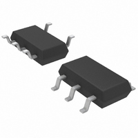
LTC1669-1CS5#TRMPBF Linear Technology, LTC1669-1CS5#TRMPBF Datasheet - Page 6

LTC1669-1CS5#TRMPBF
Manufacturer Part Number
LTC1669-1CS5#TRMPBF
Description
IC DAC 10BIT R-R I2C TSOT23-5
Manufacturer
Linear Technology
Datasheet
1.LTC1669CMS8PBF.pdf
(16 pages)
Specifications of LTC1669-1CS5#TRMPBF
Settling Time
30µs
Number Of Bits
10
Data Interface
I²C
Number Of Converters
1
Voltage Supply Source
Single Supply
Power Dissipation (max)
630µW
Operating Temperature
0°C ~ 70°C
Mounting Type
Surface Mount
Package / Case
TSOT-23-5, TSOT-5, TSOP-5
Number Of Channels
1
Resolution
10b
Interface Type
Serial (2-Wire/I2C)
Single Supply Voltage (typ)
3.3/5V
Dual Supply Voltage (typ)
Not RequiredV
Power Supply Requirement
Single
Output Type
Voltage
Integral Nonlinearity Error
±2.5LSB
Single Supply Voltage (min)
2.7V
Single Supply Voltage (max)
5.5V
Dual Supply Voltage (min)
Not RequiredV
Dual Supply Voltage (max)
Not RequiredV
Operating Temp Range
0C to 70C
Operating Temperature Classification
Commercial
Mounting
Surface Mount
Pin Count
5
Package Type
TSOT-23
Lead Free Status / RoHS Status
Lead free / RoHS Compliant
Other names
LTC1669-1CS5#PBF
LTC1669-1CS5#PBF
LTC1669-1CS5#PBF
Available stocks
Company
Part Number
Manufacturer
Quantity
Price
LTC1669
PIN FUNCTIONS
SDA (Pin 1, Pin 1 on SOT-23): Serial Data Bidirectional
Pin. Data is shifted into the SDA pin and acknowledged
by the SDA pin. High impedance pin while data is shifted
in. Open-drain N-channel output during acknowledgment.
Requires a pull-up resistor or current source to V
AD1 (Pin 2): Slave Address Select Bit 1. Tie this pin to
either V
LTC1669’s slave address.
AD2 (Pin 3): Slave Address Select Bit 2. Tie this pin to
either V
LTC1669’s slave address.
6
CC
CC
or GND to modify the corresponding bit of the
or GND to modify the corresponding bit of the
CC
.
SCL (Pin 4, Pin 5 on SOT-23): Serial Clock Input Pin.
Data is shifted into the SDA pin at the rising edges of the
clock. This high impedance pin requires a pull-up resistor
or current source to V
V
≤ 5.5V. Also used as the reference voltage input when the
part is programmed to use V
AD0 (Pin 6): Slave Address Select Bit 0. Tie this pin to
either V
LTC1669’s slave address.
GND (Pin 7, Pin 2 on SOT-23): System Ground.
V
rail-to-rail DAC output.
CC
OUT
(Pin 5, Pin 4 on SOT-23): Power Supply. 2.7V ≤ V
(Pin 8, Pin 3 on SOT-23): Voltage Output. Buffered
CC
or GND to modify the corresponding bit of the
CC
.
CC
as the reference.
1669fa
CC


