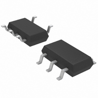
LTC1669-1CS5#TRMPBF Linear Technology, LTC1669-1CS5#TRMPBF Datasheet - Page 3

LTC1669-1CS5#TRMPBF
Manufacturer Part Number
LTC1669-1CS5#TRMPBF
Description
IC DAC 10BIT R-R I2C TSOT23-5
Manufacturer
Linear Technology
Datasheet
1.LTC1669CMS8PBF.pdf
(16 pages)
Specifications of LTC1669-1CS5#TRMPBF
Settling Time
30µs
Number Of Bits
10
Data Interface
I²C
Number Of Converters
1
Voltage Supply Source
Single Supply
Power Dissipation (max)
630µW
Operating Temperature
0°C ~ 70°C
Mounting Type
Surface Mount
Package / Case
TSOT-23-5, TSOT-5, TSOP-5
Number Of Channels
1
Resolution
10b
Interface Type
Serial (2-Wire/I2C)
Single Supply Voltage (typ)
3.3/5V
Dual Supply Voltage (typ)
Not RequiredV
Power Supply Requirement
Single
Output Type
Voltage
Integral Nonlinearity Error
±2.5LSB
Single Supply Voltage (min)
2.7V
Single Supply Voltage (max)
5.5V
Dual Supply Voltage (min)
Not RequiredV
Dual Supply Voltage (max)
Not RequiredV
Operating Temp Range
0C to 70C
Operating Temperature Classification
Commercial
Mounting
Surface Mount
Pin Count
5
Package Type
TSOT-23
Lead Free Status / RoHS Status
Lead free / RoHS Compliant
Other names
LTC1669-1CS5#PBF
LTC1669-1CS5#PBF
LTC1669-1CS5#PBF
Available stocks
Company
Part Number
Manufacturer
Quantity
Price
ELECTRICAL CHARACTERISTICS
ture range, otherwise specifi cations are at T
SYMBOL
DAC
DNL
INL
V
V
FSE
V
V
PSRR
Power Supply
V
I
I
Op Amp DC Performance
AC Performance
Digital Inputs SCL, SDAs
V
V
V
I
C
Digital Output SDA
V
CC
SD
LEAK
OS
OSTC
OUT
FSTC
CC
IH
IL
LTH
IN
OL
PARAMETER
Resolution
Monotonicity
Differential Nonlinearity
Integral Nonlinearity
Offset Error
Offset Error Temperature Coeffi cient
Full-Scale Error
DAC Output Span
Full-Scale Voltage Temperature
Coeffi cient
Power Supply Rejection Ratio
Positive Supply Voltage
Supply Current
Supply Current in Shutdown Mode
Short-Circuit Current (Sourcing)
Short-Circuit Current (Sinking)
Output Impedance to GND
Output Impedance to V
Voltage Output Slew Rate
Voltage Output Settling Time
Digital Feedthrough
Digital-to-Analog Glitch Impulse
High Level Input Voltage
Low Level Input Voltage
Logic Threshold Voltage
Digital Input Leakage
Digital Input Capacitance
Digital Output Low Voltage
CC
A
= 25°C. V
CONDITIONS
(Note 2)
Guaranteed Monotonic (Note 2)
(Note 2)
Measured at Code 20
Reference Set to V
Reference Set to Internal Bandgap
Reference Set to V
Reference Set to Internal Bandgap
Reference Set to V
Reference Set to Internal Bandgap
Reference Set to Internal Bandgap,
Code = 1023
V
V
(Note 3)
V
V
Input Code = 0, V
Input Code = 0, V
In Shutdown Mode
Input Code = 1023, V
Input Code = 1023, V
Rising (Notes 4, 5)
Falling (Notes 4, 5)
To ±0.5LSB (Notes 4, 5)
1LSB Change Around Major Carry
V
(Note 7)
I
PULLUP
CC
CC
OUT
OUT
CC
= 3V (Note 3)
= 5V (Note 3)
= 5.5V and 0V, V
Shorted to GND, Input Code = 1023
Shorted to V
CC
= 3mA
= 2.7V to 5.5V, V
The
●
CC
CC
CC
denotes specifi cations which apply over the full operating tempera-
CC
CC
CC
, Input Code = 0
= 5V
= 5V
IN
CC
CC
= GND to V
= 5V
= 5V
CC
set as reference, V
CC
l
l
l
l
l
l
l
l
l
l
l
l
l
l
l
l
l
l
OUT
MIN
2.7
2.1
10
10
unloaded, unless otherwise noted.
0 to V
0 to 2.5
± 0.2
±0.5
±0.4
0.75
0.25
0.75
TYP
±10
±15
±30
±50
150
500
120
1.8
±3
±3
60
75
12
25
30
65
80
30
70
CC
LTC1669
±0.75
MAX
± 2.5
±30
±15
±15
100
125
100
120
5.5
1.5
0.4
24
±1
10
UNITS
LSB/V
μV/°C
μV/°C
μV/°C
1669fa
3
nV•s
nV•s
V/μs
V/μs
LSB
LSB
LSB
LSB
Bits
Bits
mV
mA
mA
kΩ
μA
μA
μA
μA
μs
pF
Ω
Ω
Ω
Ω
V
V
V
V
V
V
V


