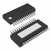
MAX5183BEEI+ Maxim Integrated Products, MAX5183BEEI+ Datasheet - Page 11

MAX5183BEEI+
Manufacturer Part Number
MAX5183BEEI+
Description
IC DAC 10BIT 40MHZ DUAL 28-QSOP
Manufacturer
Maxim Integrated Products
Datasheet
1.MAX5183BEEI.pdf
(14 pages)
Specifications of MAX5183BEEI+
Settling Time
25µs
Number Of Bits
10
Data Interface
Parallel
Number Of Converters
2
Voltage Supply Source
Analog and Digital
Operating Temperature
-40°C ~ 85°C
Mounting Type
Surface Mount
Package / Case
28-QSOP
Number Of Dac Outputs
2
Resolution
10 bit
Interface Type
Parallel
Supply Voltage (max)
3.3 V
Supply Voltage (min)
2.7 V
Maximum Operating Temperature
+ 85 C
Mounting Style
SMD/SMT
Maximum Power Dissipation
725 mW
Minimum Operating Temperature
- 40 C
Supply Current
4.2 mA
Lead Free Status / RoHS Status
Lead free / RoHS Compliant
Power Dissipation (max)
-
Lead Free Status / Rohs Status
Lead free / RoHS Compliant
the clock, the input data for DAC2 is preloaded into a
latch. On the rising edge of the clock, input data for
DAC1 is loaded to the DAC1 register, and the pre-
loaded DAC2 data in the latch is loaded to the DAC2
register.
The MAX5180 outputs are designed to supply full-scale
output currents of 1mA into 400Ω loads in parallel with
a capacitive load of 5pF. The MAX5183 features inte-
grated 400Ω resistors that restore the array currents to
proportional, differential voltages of 400mV. These dif-
ferential output voltages can then be used to drive a
balun transformer or a low-distortion, high-speed oper-
ational amplifier to convert the differential voltage into a
single-ended voltage.
Integral nonlinearity is the deviation of the values on an
actual transfer function from either a best straight-line fit
(closest approximation to the actual transfer curve) or a
line drawn between the end points of the transfer func-
tion, once offset and gain errors have been nullified.
The MAX5180/MAX5183 use a straight-line end-point fit
for INL (and DNL) and the deviations are measured at
every individual step.
Differential nonlinearity is the difference between an
actual step height and the ideal value of 1 LSB. A DNL
error specification no more negative than -1 LSB guar-
antees a monotonic transfer function.
The offset error is the difference between the ideal and
the actual offset current/voltage. For the MAX5180/
MAX5183, the offset error is the midpoint value of the
transfer function determined by the end points of a
straight-line end-point fit. This error affects all codes by
the same amount.
Gain error is the difference between the ideal and the
actual output value range. This range represents the
output when all digital inputs are set to 1 minus the out-
put when all digital inputs are set to zero.
A glitch is generated when a DAC switches between
two codes. The largest glitch is usually generated
Static and Dynamic Performance
Applications Information
______________________________________________________________________________________
Differential Nonlinearity (DNL)
Dual, 10-Bit, 40MHz, Current/Voltage
Integral Nonlinearity (INL)
Glitch Impulse
Definitions
Offset Error
Gain Error
Outputs
Simultaneous-Output DACs
around the midscale transition when the input pattern
transitions from 011…111 to 100…000. This occurs due
to timing variations between the bits. The glitch impulse
is found by integrating the voltage of the glitch at the
midscale transition over time. The glitch impulse is usu-
ally specified in pV-s.
The settling time is the amount of time required from the
start of a transition until the DAC output settles its new
output value to within the converter’s specified accuracy.
Digital feedthrough is the noise generated on a DAC’s
output when any digital input transitions. Proper board
layout and grounding will significantly reduce this
noise, but there will always be some feedthrough
caused by the DAC itself.
Total harmonic distortion (THD) is the ratio of the RMS
sum of the input signal’s first four harmonics to the fun-
damental itself. This is expressed as:
where V
V
harmonics.
SFDR is the ratio of RMS amplitude of the carrier fre-
quency (maximum signal component) to the RMS value
of the next-largest noise or harmonic distortion compo-
nent. SFDR is usually measured in dBc with respect to
the carrier frequency amplitude or in dBFS with respect
to the DAC’s full-scale range. Depending on its test
condition, SFDR is observed within a predefined win-
dow or to Nyquist. In the case of the MAX5180/MAX5183,
the SFDR performance is measured for a 0dBFS output
amplitude and analyzed within the Nyquist window.
The MAX4108 low-distortion, high-input bandwidth
amplifier may be used to generate a voltage from the
array current output of the MAX5180. The differential
voltage across OUT1P (or OUT2P) and OUT1N (or
OUT2N) is converted into a single-ended voltage by
designing an appropriate operational amplifier configu-
ration
5
are the amplitudes of the 2nd- through 5th-order
Differential to Single-Ended Conversion
(Figure
THD
1
is the fundamental amplitude, and V
=
5).
20
Spurious-Free Dynamic Range (SFDR)
×
log
V
2
2
+
Total Harmonic Distortion
V
3
2
V
+
1
V
Digital Feedthrough
4
2
+
V
5
Settling Time
2
2
through
11


