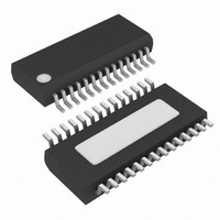
MAX5183BEEI+ Maxim Integrated Products, MAX5183BEEI+ Datasheet

MAX5183BEEI+
Specifications of MAX5183BEEI+
Related parts for MAX5183BEEI+
MAX5183BEEI+ Summary of contents
Page 1
... Signal Reconstruction of I and Q Transmit Signals Digital Signal Processing Arbitrary Waveform Generation (AWG) Imaging ________________________________________________________________ Maxim Integrated Products For pricing, delivery, and ordering information, please contact Maxim/Dallas Direct! at 1-888-629-4642, or visit Maxim’s website at www.maxim-ic.com. Simultaneous-Output DACs 2.7V to 3.3V Single-Supply Operation Wide Spurious-Free Dynamic Range: 70dB ...
Page 2
Dual, 10-Bit, 40MHz, Current/Voltage Simultaneous-Output DACs ABSOLUTE MAXIMUM RATINGS AGND, DGND .................................-0. Digital Inputs to DGND.............................................-0.3V to +6V OUT1P, OUT1N, OUT2P, OUT2N, CREF1, CREF2 to AGND ...................................................-0. AGND ...
Page 3
Dual, 10-Bit, 40MHz, Current/Voltage ELECTRICAL CHARACTERISTICS (continued) ( ±10%, AGND = DGND = unless otherwise noted. Typical values are at T PARAMETER SYMBOL REFERENCE Output Voltage Range V Output Voltage Temperature TCV ...
Page 4
Dual, 10-Bit, 40MHz, Current/Voltage Simultaneous-Output DACs ( 3V, AGND = DGND = 0, 400Ω differential output INTEGRAL NONLINEARITY vs. INPUT CODE 0.6 0.5 0.4 0.3 0.2 0.1 0 -0.1 -0.2 0 128 256 384 ...
Page 5
Dual, 10-Bit, 40MHz, Current/Voltage ( 3V, AGND = DGND = 0, 400Ω differential output INTERNAL REFERENCE VOLTAGE vs. SUPPLY VOLTAGE 1.28 1.27 1.26 MAX5180 1.25 MAX5183 1.24 1.23 2.5 3.0 3.5 4.0 4.5 5.0 ...
Page 6
Dual, 10-Bit, 40MHz, Current/Voltage Simultaneous-Output DACs ( 3V, AGND = DGND = 0, 400Ω differential output SPURIOUS-FREE DYNAMIC RANGE vs. OUTPUT FREQUENCY AND CLOCK FREQUENCY, DAC1 60MHz CLK f = ...
Page 7
Dual, 10-Bit, 40MHz, Current/Voltage ______________________________________________________________Pin Description PIN NAME 1 CREF1 Reference Bias Bypass, DAC1 2 OUT1P Positive Analog Output, DAC1. Current output for MAX5180; voltage output for MAX5183. 3 OUT1N Negative Analog Output, DAC1. Current output for MAX5180; voltage output ...
Page 8
Dual, 10-Bit, 40MHz, Current/Voltage Simultaneous-Output DACs 1.2V REF REFO REFR * 9.6k CLK *INTERNAL 400Ω AND 9.6kΩ RESISTORS FOR MAX5183 ONLY. Figure 1. Functional Diagram Detailed Description The MAX5180/MAX5183 are dual, 10-bit digital-to-ana- log converters (DACs) capable of operating with ...
Page 9
Dual, 10-Bit, 40MHz, Current/Voltage OPTIONAL EXTERNAL BUFFER FOR HEAVIER LOADS MAX4040 AGND V REF I = REF R SET *COMPENSATION CAPACITOR (C ≈ 100nF). COMP **9.6kΩ REFERENCE CURRENT-SET RESISTOR INTERNAL TO MAX5183 ONLY. USE EXTERNAL R FOR MAX5180. SET Figure ...
Page 10
Dual, 10-Bit, 40MHz, Current/Voltage Simultaneous-Output DACs External Reference To disable the MAX5180/MAX5183’s internal reference, connect REN temperature-stable, external DD reference may now be applied to drive the REFO pin to set the full-scale output (Figure 3). ...
Page 11
Dual, 10-Bit, 40MHz, Current/Voltage the clock, the input data for DAC2 is preloaded into a latch. On the rising edge of the clock, input data for DAC1 is loaded to the DAC1 register, and the pre- loaded DAC2 data in ...
Page 12
Dual, 10-Bit, 40MHz, Current/Voltage Simultaneous-Output DACs 3V 3V 10µF 0.1µ CLK D0–D9 REFO 0.1µF REFR R ** SET DGND Figure 5. Differential to Single-Ended Conversion Using a Low-Distortion Amplifier I/Q Reconstruction in a QAM Application The MAX5180/MAX5183’s low-distortion ...
Page 13
Dual, 10-Bit, 40MHz, Current/Voltage 3V DIGITAL SIGNAL PROCESSOR Figure 6. Using the MAX5180/MAX5183 for I/Q Signal Reconstruction grounding and power-supply decoupling guidelines for high-speed, high-frequency applications should be closely followed. First, a multilayer pc board with separate ground and power-supply ...
Page 14
... Maxim cannot assume responsibility for use of any circuitry other than circuitry entirely embodied in a Maxim product. No circuit patent licenses are implied. Maxim reserves the right to change the circuitry and specifications without notice at any time. 14 ____________________Maxim Integrated Products, 120 San Gabriel Drive, Sunnyvale, CA 94086 408-737-7600 © 2003 Maxim Integrated Products Printed USA is a registered trademark of Maxim Integrated Products ...


