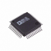
AD7839ASZ Analog Devices Inc, AD7839ASZ Datasheet - Page 9

AD7839ASZ
Manufacturer Part Number
AD7839ASZ
Description
IC DAC 13BIT OCTAL V-OUT 44-MQFP
Manufacturer
Analog Devices Inc
Datasheet
1.AD7839ASZ.pdf
(12 pages)
Specifications of AD7839ASZ
Data Interface
Parallel
Settling Time
30µs
Number Of Bits
13
Number Of Converters
8
Voltage Supply Source
Analog and Digital, Dual ±
Power Dissipation (max)
303mW
Operating Temperature
-40°C ~ 85°C
Mounting Type
Surface Mount
Package / Case
44-MQFP, 44-PQFP
Resolution (bits)
13bit
Sampling Rate
33kSPS
Input Channel Type
Parallel
Supply Current
8mA
Digital Ic Case Style
QFP
No. Of Pins
44
Number Of Channels
8
Resolution
13b
Conversion Rate
33KSPS
Interface Type
Parallel
Single Supply Voltage (typ)
Not RequiredV
Dual Supply Voltage (typ)
±15V
Architecture
R-2R
Power Supply Requirement
Dual
Output Type
Voltage
Integral Nonlinearity Error
±2LSB
Single Supply Voltage (min)
Not RequiredV
Single Supply Voltage (max)
Not RequiredV
Dual Supply Voltage (min)
±14.25V
Dual Supply Voltage (max)
±15.75V
Operating Temp Range
-40C to 85C
Operating Temperature Classification
Industrial
Mounting
Surface Mount
Pin Count
44
Package Type
MQFP
Lead Free Status / RoHS Status
Lead free / RoHS Compliant
For Use With
EVAL-AD7839EBZ - BOARD EVAL FOR AD7839
Lead Free Status / Rohs Status
Compliant
Available stocks
Company
Part Number
Manufacturer
Quantity
Price
Company:
Part Number:
AD7839ASZ
Manufacturer:
Analog Devices Inc
Quantity:
10 000
Part Number:
AD7839ASZ
Manufacturer:
ADI/亚德诺
Quantity:
20 000
Company:
Part Number:
AD7839ASZ-REEL
Manufacturer:
Analog Devices Inc
Quantity:
10 000
Power-On with CLR Low
The output stage of the AD7839 has been designed to allow
output stability during power-on. If CLR is kept low during
power-on, then just after power is applied to the AD7839, the
situation is as depicted in Figure 14. G
while G
V
G
parallel with the gain resistors of the output amplifier. The
output amplifier is connected as a unity gain buffer via G
the DUTGND voltage is applied to the buffer input via G
amplifier’s output is thus at the same voltage as the DUTGND
pin. The output stage remains configured as in Figure 14 until
the voltage at V
–3 V. By now the output amplifier has enough headroom to
handle signals at its input and has also had time to settle. The
internal power-on circuitry opens G
G
fier is configured in its noise gain configuration via G
The DUTGND voltage is still connected to the noninverting
input via G
V
opening of G
via the configuration shown in Figure 15.
When CLR is taken back high, the output stage is configured as
shown in Figure 16. The internal control logic closes G
opens G
gain-of-two configuration. The voltage that appears on the V
pins is determined by the data present in the DAC registers.
REV. 0
OUT
OUT
Figure 14. Output Stage with V
CLR Low
5
6
Figure 15. Output Stage with V
CLR Low
. This situation is shown in Figure 15. Now the output ampli-
and a 14 k resistor. This thin-film resistor is connected in
is kept within a few hundred millivolts of DUTGND via
has been disconnected from the DUTGND pin by the
2
DAC
DAC
2
, G
. The output amplifier is connected in a noninverting
2
3
and this voltage appears at V
5
and G
, but will track the voltage present at DUTGND
DD
G
G
G
G
1
1
2
exceeds 7 V and V
2
5
are closed.
DUTGND
DUTGND
R
R
G
G
4
4
G
G
G
G
3
5
3
5
R
R
3
DD
14k
DD
14k
and G
SS
1
< 7 V or V
> 7 V and V
, G
G
G
is more negative than
6
OUT
6
4
5
and G
and closes G
.
SS
6
SS
are open
> –3 V;
4
V
V
OUT
and G
OUT
< –3 V;
1
2
. The
and
3
, and
4
and
OUT
6
.
–9–
Power-On with CLR High
If CLR is high on the application of power to the device, the
output stages of the AD7839 are configured as in Figure 17
while V
G
DAC to the input of its output amplifier. G
while G
a unity gain buffer. V
through a 14 k resistor until V
negative than –3 V.
When the difference between the supply voltages reaches +10 V,
the internal power-on circuitry opens G
and G
1
Figure 18. Output Stage Powering Up with CLR High;
V
Figure 17. Output Stage Powering Up with CLR High
While V
is closed and G
DD
Figure 16. Output Stage After CLR Is Taken High
6
> 7 V and V
DD
4
configuring the output stage as shown in Figure 18.
DAC
DAC
DAC
and G
is less than 7 V and V
DD
< 7 V or V
6
are open, thus connecting the output amplifier as
G
G
G
G
2
G
G
1
1
1
SS
2
2
is open, thereby connecting the output of the
2
OUT
< –3 V
DUTGND
DUTGND
DUTGND
R
R
R
SS
is connected to DUTGND via G
> –3 V
G
G
G
4
4
4
SS
DD
G
G
G
G
G
G
3
5
3
5
3
5
is more positive than –3 V.
exceeds 7 V and V
R
R
R
14k
14k
14k
3
G
G
G
and G
6
6
6
3
and G
5
AD7839
and closes G
5
are closed
V
V
V
SS
OUT
OUT
OUT
is more
5
4


