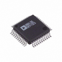
AD7839ASZ Analog Devices Inc, AD7839ASZ Datasheet - Page 3

AD7839ASZ
Manufacturer Part Number
AD7839ASZ
Description
IC DAC 13BIT OCTAL V-OUT 44-MQFP
Manufacturer
Analog Devices Inc
Datasheet
1.AD7839ASZ.pdf
(12 pages)
Specifications of AD7839ASZ
Data Interface
Parallel
Settling Time
30µs
Number Of Bits
13
Number Of Converters
8
Voltage Supply Source
Analog and Digital, Dual ±
Power Dissipation (max)
303mW
Operating Temperature
-40°C ~ 85°C
Mounting Type
Surface Mount
Package / Case
44-MQFP, 44-PQFP
Resolution (bits)
13bit
Sampling Rate
33kSPS
Input Channel Type
Parallel
Supply Current
8mA
Digital Ic Case Style
QFP
No. Of Pins
44
Number Of Channels
8
Resolution
13b
Conversion Rate
33KSPS
Interface Type
Parallel
Single Supply Voltage (typ)
Not RequiredV
Dual Supply Voltage (typ)
±15V
Architecture
R-2R
Power Supply Requirement
Dual
Output Type
Voltage
Integral Nonlinearity Error
±2LSB
Single Supply Voltage (min)
Not RequiredV
Single Supply Voltage (max)
Not RequiredV
Dual Supply Voltage (min)
±14.25V
Dual Supply Voltage (max)
±15.75V
Operating Temp Range
-40C to 85C
Operating Temperature Classification
Industrial
Mounting
Surface Mount
Pin Count
44
Package Type
MQFP
Lead Free Status / RoHS Status
Lead free / RoHS Compliant
For Use With
EVAL-AD7839EBZ - BOARD EVAL FOR AD7839
Lead Free Status / Rohs Status
Compliant
Available stocks
Company
Part Number
Manufacturer
Quantity
Price
Company:
Part Number:
AD7839ASZ
Manufacturer:
Analog Devices Inc
Quantity:
10 000
Part Number:
AD7839ASZ
Manufacturer:
ADI/亚德诺
Quantity:
20 000
Company:
Part Number:
AD7839ASZ-REEL
Manufacturer:
Analog Devices Inc
Quantity:
10 000
AC PERFORMANCE CHARACTERISTICS
Parameter
DYNAMIC PERFORMANCE
Specifications subject to change without notice.
TIMING SPECIFICATIONS
Parameter
t
t
t
t
t
t
t
t
t
t
t
NOTES
1
2
Specifications subject to change without notice.
REV. 0
All input signals are specified with tr = tf = 5 ns (10% to 90% of 5 V) and timed from a voltage level of 1.6 V.
Rise and fall times should be no longer than 50 ns.
1
2
3
4
5
6
7
8
9
10
11
Output Voltage Settling Time
Slew Rate
Digital-to-Analog Glitch Impulse
Channel-to-Channel Isolation
DAC-to-DAC Crosstalk
Digital Crosstalk
Digital Feedthrough
Output Noise Spectral Density
@ 1 kHz
Limit at T
15
0
50
50
0
0
20
0
30
300
50
A0, A1, A2
DATA
LDAC
V
V
CLR
OUT
OUT
WR
CS
MIN,
1, 2
A
30
40
0.7
230
99
40
0.2
0.1
200
T
t
t
1
5
MAX
(V
CC
t
t
3
4
t
Units
V/ s typ
nV-s typ
dB typ
nV-s typ
nV-s typ
nV-s typ
nV/ Hz typ
= +5 V
7
s typ
s max
t
10
t
t
t
2
6
8
Figure 1. Timing Diagram
t
9
5%; V
(These characteristics are included for Design Guidance and are not subject
to production testing.)
DD
Test Conditions/Comments
Full-Scale Change to 1/2 LSB. DAC Latch Contents Alternately
Loaded with All 0s and All 1s
Measured with V
Alternately Loaded with 0FFF Hex and 1000 Hex. Not Dependent
on Load Conditions
See Terminology
See Terminology
Feedthrough to DAC Output Under Test Due to Change in Digital
Input Code to Another Converter
Effect of Input Bus Activity on DAC Output Under Test
All 1s Loaded to DAC. V
Units
ns min
ns min
ns min
ns min
ns min
ns min
ns min
ns min
ns max
ns min
= +15 V
s typ
–3–
5%; V
REF
SS
= –15 V
(+) = +5 V, V
REF
(+) = V
5%; GND = DUTGND = 0 V)
t
11
REF
Description
Address to WR Setup Time
Address to WR Hold Time
CS Pulsewidth Low
WR Pulsewidth Low
CS to WR Setup Time
WR to CS Hold Time
Data Setup Time
Data Hold Time
Settling Time
CLR Pulse Activation Time
LDAC Pulsewidth Low
REF
(–) = –5 V. DAC Latch
(–) = 0 V
AD7839


