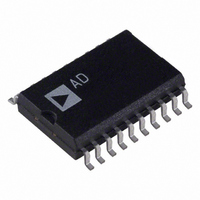
AD7392ARZ Analog Devices Inc, AD7392ARZ Datasheet - Page 7

AD7392ARZ
Manufacturer Part Number
AD7392ARZ
Description
IC DAC 12BIT PARALLEL 3V 20-SOIC
Manufacturer
Analog Devices Inc
Datasheet
1.AD7392ARZ.pdf
(20 pages)
Specifications of AD7392ARZ
Data Interface
Parallel
Settling Time
60µs
Number Of Bits
12
Number Of Converters
1
Voltage Supply Source
Single Supply
Power Dissipation (max)
500µW
Operating Temperature
-40°C ~ 85°C
Mounting Type
Surface Mount
Package / Case
20-SOIC (7.5mm Width)
Resolution (bits)
12bit
Sampling Rate
17kSPS
Input Channel Type
Parallel
Supply Voltage Range - Analogue
2.7V To 5.5V
Supply Current
55µA
Digital Ic Case Style
SOIC
Number Of Channels
1
Resolution
12b
Conversion Rate
17KSPS
Interface Type
Parallel
Single Supply Voltage (typ)
3V
Dual Supply Voltage (typ)
Not RequiredV
Architecture
R-2R
Power Supply Requirement
Single
Output Type
Voltage
Single Supply Voltage (min)
2.7V
Single Supply Voltage (max)
5.5V
Dual Supply Voltage (min)
Not RequiredV
Dual Supply Voltage (max)
Not RequiredV
Operating Temp Range
-40C to 85C
Operating Temperature Classification
Industrial
Mounting
Surface Mount
Pin Count
20
Lead Free Status / RoHS Status
Lead free / RoHS Compliant
Lead Free Status / RoHS Status
Lead free / RoHS Compliant, Lead free / RoHS Compliant
Available stocks
Company
Part Number
Manufacturer
Quantity
Price
Company:
Part Number:
AD7392ARZ
Manufacturer:
ON
Quantity:
4 522
Part Number:
AD7392ARZ
Manufacturer:
ADI/亚德诺
Quantity:
20 000
Part Number:
AD7392ARZ-REEL
Manufacturer:
ADI/亚德诺
Quantity:
20 000
PIN CONFIGURATIONS AND FUNCTION DESCRIPTIONS
Table 4. AD7392 Pin Function Descriptions
Pin No.
1
2
3
4
5 to 16
17
18
19
20
Table 5. AD7393 Pin Function Descriptions
Pin No.
1
2
3
4
5, 6
7 to 16
17
18
19
20
Mnemonic
V
SHDN
CS
RS
D0 to D11
DGND
AGND
V
V
Mnemonic
V
SHDN
CS
RS
NC
D0 to D9
DGND
AGND
V
V
DD
OUT
REF
DD
OUT
REF
Figure 3. AD7392 Pin Configuration
SHDN
V
CS
RS
DD
D0
D1
D2
D3
D4
D5
Description
Positive Power Supply Input. The specified range of operation is 2.7 V to 5.5 V.
Power Shutdown Active Low Input. DAC register contents are saved as long as power stays on the V
SHDN = 0, CS strobes write new data into the DAC register.
Chip Select Latch Enable, Active Low.
Asynchronous Active Low Input. Resets the DAC register to 0.
Parallel Input Data Bits. D11 is the MSB; D0 is the LSB.
Digital Ground.
Analog Ground.
DAC Voltage Output.
DAC Reference Input. Establishes the DAC full-scale voltage.
10
Description
Positive Power Supply Input. The specified range of operation is 2.7 V to 5.5 V.
Power Shutdown Active Low Input. DAC register contents are saved as long as power stays on the V
When SHDN = 0, CS strobes write new data into the DAC register.
Chip Select Latch Enable, Active Low.
Asynchronous Active Low Input. Resets the DAC register to 0.
No Connect.
Parallel Input Data Bits. D9 is the MSB; D0 is the LSB.
Digital Ground.
Analog Ground.
DAC Voltage Output.
DAC Reference Input. Establishes the DAC full-scale voltage.
1
2
3
4
5
6
7
8
9
(Not to Scale)
AD7392
TOP VIEW
20
19
18
17
16
15
14
13
12
11
V
V
AGND
DGND
D11
D10
D9
D8
D7
D6
REF
OUT
Rev. C | Page 7 of 20
Figure 4. AD7393 Pin Configuration
SHDN
V
NC
NC
CS
RS
D0
D1
D2
D3
DD
10
NC = NO CONNECT
1
2
3
4
5
6
7
8
9
(Not to Scale)
AD7393
TOP VIEW
AD7392/AD7393
20
19
18
17
16
15
14
13
12
11
V
V
AGND
DGND
D9
D8
D7
D6
D5
D4
REF
OUT
DD
DD
pin. When
pin.


