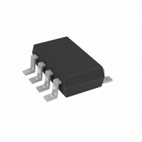
AD5165BUJZ100-R2 Analog Devices Inc, AD5165BUJZ100-R2 Datasheet - Page 13

AD5165BUJZ100-R2
Manufacturer Part Number
AD5165BUJZ100-R2
Description
IC DGTL POT 100K LP TSOT23-8
Manufacturer
Analog Devices Inc
Datasheet
1.AD5165BUJZ100-R7.pdf
(16 pages)
Specifications of AD5165BUJZ100-R2
Taps
256
Resistance (ohms)
100K
Number Of Circuits
1
Temperature Coefficient
35 ppm/°C Typical
Memory Type
Volatile
Interface
SPI, 3-Wire Serial
Voltage - Supply
2.7 V ~ 5.5 V
Operating Temperature
-40°C ~ 125°C
Mounting Type
Surface Mount
Package / Case
TSOT-23-8, TSOT-8
Resistance In Ohms
100K
End To End Resistance
100kohm
Track Taper
Linear
No. Of Steps
256
Resistance Tolerance
± 20%
Supply Voltage Range
2.7V To 5.5V
Control Interface
Serial, SPI
No. Of Pots
Single
Lead Free Status / RoHS Status
Lead free / RoHS Compliant
For Use With
EVAL-AD5165EBZ - BOARD EVALUATION FOR AD5165
Lead Free Status / RoHS Status
Lead free / RoHS Compliant, Lead free / RoHS Compliant
Other names
AD5165BUJZ100-R2
AD5165BUJZ100-R2TR
AD5165BUJZ100-R2TR
Available stocks
Company
Part Number
Manufacturer
Quantity
Price
Company:
Part Number:
AD5165BUJZ100-R2
Manufacturer:
ADI
Quantity:
13 507
AD5165
THEORY OF OPERATION
The AD5165 is a 256-position digitally controlled variable
resistor (VR) device.
PROGRAMMING THE VARIABLE RESISTOR
Rheostat Operation
The nominal resistance of the RDAC between terminals A and
B is available in 100 kΩ. The nominal resistance (R
has 256 contact points accessed by the wiper terminal, plus the
B terminal contact. The 8-bit data in the RDAC latch is decoded
to select one of the 256 possible settings.
Assuming that a 100 kΩ part is used, the wiper’s first connec-
tion starts at the B terminal for data 0x00. Because there is a
50 Ω wiper contact resistance, such a connection yields a mini-
mum of 100 Ω (2 × 50 Ω) resistance between terminals W and
B. The second connection is the first tap point, which corres-
ponds to 490 Ω (R
for data 0x01. The third connection is the next tap point,
representing 880 Ω (2 × 390 Ω + 2 × 50 Ω) for data 0x02, and
so on. Each LSB data value increase moves the wiper up the
resistor ladder until the last tap point is reached at 100,100 Ω
(R
The general equation determining the digitally programmed
output resistance between W and B is
AB
+ 2 × R
R
WB
A
B
(
D
)
W
).
=
Figure 37. AD5165 Equivalent RDAC Circuit
W
Figure 36. Rheostat Mode Configuration
D7
D6
D5
D4
D3
D2
D1
D0
256
DECODER
D
LATCH
RDAC
AND
WB
×
= R
R
AB
AB
A
B
+
/256 + 2 × R
2
R
R
R
R
×
S
S
S
S
R
W
W
W
= 390 Ω + 2 × 50 Ω)
A
B
A
W
B
W
AB
) of the VR
(1)
Rev. 0 | Page 13 of 16
where:
D is the decimal equivalent of the binary code loaded in the
R
R
In summary, if R
circuited, the following output resistance R
indicated RDAC latch codes.
Table 6. Codes and Corresponding R
D (Dec.)
255
128
1
0
Note that, in the zero-scale condition, a finite wiper resistance
of 100 Ω is present. Care should be taken to limit the current
flow between W and B in this state to a maximum pulse current
of no more than 20 mA. Otherwise, degradation or possible
destruction of the internal switch contact can occur.
Similar to the mechanical potentiometer, the resistance of the
RDAC between the wiper W and terminal A also produces a
digitally controlled complementary resistance, R
terminals are used, the B terminal can be opened. Setting the
resistance value for R
and decreases as the data loaded in the latch increases in value.
The general equation for this operation is
For R
following output resistance R
latch codes.
Table 7. Codes and Corresponding R
D (Dec.)
255
128
1
0
Typical device-to-device matching is process-lot dependent
and may vary by up to ±20%. Because the resistance element
is processed in thin film technology, the change in R
temperature has a very low 35 ppm/°C temperature coefficient.
AB
W
8-bit RDAC register.
the internal switch.
is the wiper resistance contributed by the on resistance of
is the end-to-end resistance.
R
AB
WA
= 100 kΩ with the B terminal open circuited, the
(
D
)
R
99,710
50,100
490
100
=
WB
256
(Ω)
AB
256
R
490
50,100
99, 710
100,100
= 100 kΩ and the A terminal is open
WA
−
WA
D
(Ω)
Output State
Full scale (R
Midscale
1 LSB
Zero scale (wiper contact resistance)
starts at a maximum value of resistance
×
R
AB
WA
+
2
is set for the indicated RDAC
×
AB
R
Output State
Full scale
Midscale
1 LSB
Zero scale
W
– 1 LSB + R
WB
WA
Resistance
Resistance
WB
is set for the
W
WA
)
. When these
AB
with
(2)


