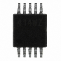
ISL22414WFU10Z Intersil, ISL22414WFU10Z Datasheet - Page 6

ISL22414WFU10Z
Manufacturer Part Number
ISL22414WFU10Z
Description
IC POT DGTL 256TP LN LP 10-MSOP
Manufacturer
Intersil
Series
XDCP™r
Datasheet
1.ISL22414WFU10Z.pdf
(16 pages)
Specifications of ISL22414WFU10Z
Taps
256
Resistance (ohms)
10K
Number Of Circuits
1
Temperature Coefficient
±50ppm/°C
Memory Type
Non-Volatile
Interface
SPI Serial
Voltage - Supply
±2.25 V ~ 5.5 V
Operating Temperature
-40°C ~ 125°C
Mounting Type
Surface Mount
Package / Case
10-MSOP, Micro10™, 10-uMAX, 10-uSOP
Resistance In Ohms
10K
Lead Free Status / RoHS Status
Lead free / RoHS Compliant
Available stocks
Company
Part Number
Manufacturer
Quantity
Price
Company:
Part Number:
ISL22414WFU10Z
Manufacturer:
Intersil
Quantity:
500
Company:
Part Number:
ISL22414WFU10Z-T7A
Manufacturer:
INTERSIL
Quantity:
1 001
Operating Specifications
NOTES:
10.
12. Roffset = RW
13. RDNL = (RW
14. RINL = [RW
15.
16. t
17. R
18. Compliance to datasheet limits is assured by one or more methods: production test, characterization and/or design.
11. MI =
4. Typical values are for T
5. LSB: [V(RW)
6. ZS error = V(RW)
7. FS error = [V(RW)
8. DNL = [V(RW)
9. INL = [V(RW)
SYMBOL
(Note 17)
t
f
t
Cpin
LEAD
t
incremental voltage when changing from one tap to an adjacent tap.
00 hex respectively.
Roffset = RW
R
t
t
SCK
CYC
t
LAG
t
t
t
t
t
t
TC
WC
WH
DIS
TC
WL
t
t
HO
RO
SU
SO
FO
CS
t
t
RI
FI
pu
H
pu
V
V
R
is the time from the end of a Write sequence of SPI serial interface, to the end of the self-timed internal non-volatile write cycle.
is specified for the highest data rate transfer for the device. Higher value pull-up can be used at lower data rates.
|
RW
=
=
--------------------------------------------------------------------------------------------- -
[
--------------------------------------------------------------- -
[
255
SDO Pull-up Resistor Off-chip
Capacitance
SPI Frequency
SPI Clock Cycle Time
SPI Clock High Time
SPI Clock Low Time
Lead Time
Lag Time
SDI, SCK and CS Input Setup Time
SDI, SCK and CS Input Hold Time
SDI, SCK and CS Input Rise Time
SDI, SCK and CS Input Fall Time
SDO output Disable Time
SDO Output Setup Time
SDO Output Valid Time
SDO Output Hold Time
SDO Output Rise Time
SDO Output Fall Time
CS Deselect Time
Max V RW
Max Ri
SCK, SDI, SDO and CS Pin
[
Max V RW
Max Ri
i
255
i
– (MI • i) – RW
i
– RW
0
255
– RW
i
– i • LSB – V(RW)]/LSB for i = 1 to 255
(
/
(
MI, when measuring between RW and RL.
– V(RW)
(
(
– V(RW)
/
(
MI, when measuring between RW and RH.
0
255
)
(
/
LSB.
0
+
) Min Ri
i-1
|
–
/
PARAMETER
255. MI is a minimum increment. RW
Min Ri
)
– V
)
i
/
A
MI -1, for i = 1 to 255.
)
)
i-1
i
+
) Min V RW
= +25°C and 3.3V supply voltage.
0
(
CC
]
–
]
Min V RW
(
/
/
LSB-1, for i = 1 to 255. i is the DCP register setting.
255. V(RW)
0
]
)
]
6
/
/
LSB.
] 2 ⁄
MI, for i = 1 to 255.
)
(
]
Over the recommended operating conditions unless otherwise specified. Boldface limits apply over the
operating temperature range. (Continued)
(
(
×
(
-------------- -
ΔT°C
10
)
i
255
6
)
)
i
] 2 ⁄
)
for i = 16 to 255, T = -40°C to +125°C or T = -55°C to +125°C. Max( ) is the maximum value of the
resistance and Min( ) is the minimum value of the resistance over the temperature range.
and V(RW)
×
-------------- -
ΔT°C
10
Maximum is determined by t
maximum bus load Cb = 30pF, f
R
R
pu
pu
6
= 2k, Cbus = 30pF
= 2k, Cbus = 30pF
for i = 16 to 255 decimal, T = -40°C to +125°C or T = -55°C to +125°C. Max( ) is the
maximum value of the wiper voltage and Min ( ) is the minimum value of the wiper voltage
over the temperature range.
0
are V(RW) for the DCP register set to FF hex and 00 hex respectively. LSB is the
255
ISL22414
TEST CONDITIONS
and RW
0
are the measured resistances for the DCP register set to FF hex and
RO
SCK
and t
= 5MHz
FO
with
(Note 18)
MIN
200
100
100
250
250
150
50
50
10
10
50
0
0
2
(Note 4)
TYP
10
(Note 18)
MAX
100
20
60
60
2
5
December 16, 2010
UNIT
FN6424.1
MHz
kΩ
pF
ns
ns
ns
ns
ns
ns
ns
ns
ns
ns
ns
ns
ns
ns
ns
µs


