AD7874BNZ Analog Devices Inc, AD7874BNZ Datasheet - Page 4
AD7874BNZ
Manufacturer Part Number
AD7874BNZ
Description
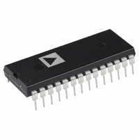
IC DAS 12BIT 4CH 5V 28-DIP
Manufacturer
Analog Devices Inc
Type
Data Acquisition System (DAS)r
Datasheet
1.AD7874ARZ.pdf
(16 pages)
Specifications of AD7874BNZ
Resolution (bits)
12 b
Data Interface
Parallel
Sampling Rate (per Second)
116k
Voltage Supply Source
Dual ±
Voltage - Supply
5V
Operating Temperature
-40°C ~ 85°C
Mounting Type
Through Hole
Package / Case
28-DIP (0.600", 15.24mm)
Sampling Rate
116kSPS
Input Channel Type
Single Ended
Supply Voltage Range - Analog
± 4.75V To ± 5.25V
Supply Current
12mA
Lead Free Status / RoHS Status
Lead free / RoHS Compliant
Available stocks
Company
Part Number
Manufacturer
Quantity
Price


AD7874
TERMINOLOGY
ACQUISITION TIME
Acquisition Time is the time required for the output of the
track/hold amplifiers to reach their final values, within 1/2
LSB, after the falling edge of INT (the point at which the track/
holds return to track mode). This includes switch delay time,
slewing time and settling time for a full-scale voltage change.
APERTURE DELAY
Aperture Delay is defined as the time required by the internal
switches to disconnect the hold capacitors from the inputs. This
produces an effective delay in sample timing. It is measured by
applying a step input and adjusting the CONVST input position
until the output code follows the step input change.
APERTURE DELAY MATCHING
Aperture Delay Matching is the maximum deviation in aperture
delays across the four on-chip track/hold amplifiers.
APERTURE JITTER
Aperture Jitter is the uncertainty in aperture delay caused by
internal noise and variation of switching thresholds with signal
level.
DROOP RATE
Droop Rate is the change in the held analog voltage resulting
from leakage currents.
CHANNEL-TO-CHANNEL ISOLATION
Channel-to-Channel Isolation is a measure of the level of
crosstalk between channels. It is measured by applying a full-
scale 1 kHz signal to the other three inputs. The figure given is
the worst case across all four channels.
SNR, THD, IMD
See DYNAMIC SPECIFICATIONS section.
–4–
DB11 (MSB)
CONVST
DB10
DB11 (MSB)
CLK
V
RD
CS
DD
CONVST
10
DGND
11
PIN CONFIGURATIONS
DB10
5
6
7
8
9
CLK
V
V
DB9
DB8
V
V
INT
RD
IN1
IN2
CS
DD
DD
12 13
4
10
11
11
12
13
14
DIP and SOIC
1
2
3
4
5
6
7
8
9
3
(Not to Scale)
(Not to Scale)
AD7874
TOP VIEW
LCCC
AD7874
14 15
TOP VIEW
2
1 28
16
17
27
28
27
25
24
23
22
21
20
19
18
17
16
15
26
18
26
V
V
V
REF OUT
REF IN
AGND
DB0 (LSB)
DB1
DB2
DB3
DB4
DB5
DB6
DB7
IN4
IN3
SS
25
24
23
22
21
20
19
REF OUT
REF IN
AGND
DB0 (LSB)
DB1
DB2
DB3
REV. C
Related parts for AD7874BNZ
Image
Part Number
Description
Manufacturer
Datasheet
Request
R

Part Number:
Description:
±1.7g Dual-Axis IMEMS Accelerometer Evaluation Board
Manufacturer:
Analog Devices Inc
Datasheet:

Part Number:
Description:
Inertial Sensor Evaluation System
Manufacturer:
Analog Devices Inc
Datasheet:
Part Number:
Description:
Manufacturer:
Analog Devices Inc
Datasheet:
Part Number:
Description:
Manufacturer:
Analog Devices Inc
Datasheet:
Part Number:
Description:
Manufacturer:
Analog Devices Inc
Datasheet:
Part Number:
Description:
Manufacturer:
Analog Devices Inc
Datasheet:
Part Number:
Description:
Manufacturer:
Analog Devices Inc
Datasheet:
Part Number:
Description:
Manufacturer:
Analog Devices Inc
Datasheet:
Part Number:
Description:
Manufacturer:
Analog Devices Inc
Datasheet:
Part Number:
Description:
Manufacturer:
Analog Devices Inc
Datasheet:
Part Number:
Description:
Manufacturer:
Analog Devices Inc
Datasheet:
Part Number:
Description:
Manufacturer:
Analog Devices Inc
Datasheet:
Part Number:
Description:
Manufacturer:
Analog Devices Inc
Datasheet: