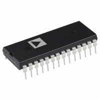
AD7874BNZ Analog Devices Inc, AD7874BNZ Datasheet - Page 11

AD7874BNZ
Manufacturer Part Number
AD7874BNZ
Description
IC DAS 12BIT 4CH 5V 28-DIP
Manufacturer
Analog Devices Inc
Type
Data Acquisition System (DAS)r
Datasheet
1.AD7874ARZ.pdf
(16 pages)
Specifications of AD7874BNZ
Resolution (bits)
12 b
Data Interface
Parallel
Sampling Rate (per Second)
116k
Voltage Supply Source
Dual ±
Voltage - Supply
5V
Operating Temperature
-40°C ~ 85°C
Mounting Type
Through Hole
Package / Case
28-DIP (0.600", 15.24mm)
Sampling Rate
116kSPS
Input Channel Type
Single Ended
Supply Voltage Range - Analog
± 4.75V To ± 5.25V
Supply Current
12mA
Lead Free Status / RoHS Status
Lead free / RoHS Compliant
Available stocks
Company
Part Number
Manufacturer
Quantity
Price
REV. C
Some applications may require that the conversion is initiated
by the microprocessor rather than an external timer. One option
is to decode the AD7874 CONVST from the address bus so
that a write operation starts a conversion. Data is read at the
end of the conversion sequence as before. Figure 16 shows an
example of initiating conversion using this method. Note that
for all interfaces, a read operation should not be attempted dur-
ing conversion.
AD7874–MC68000 Interface
An interface between the AD7874 and the MC68000 is shown
in Figure 15. As before, conversion is initiated using an external
timer. The AD7874 INT line can be used to interrupt the pro-
cessor or, alternatively, software delays can ensure that conver-
sion has been completed before a read to the AD7874 is
attempted. Because of the nature of its interrupts, the 68000
requires additional logic (not shown in Figure 15) to allow it to
be interrupted correctly. For further information on 68000 in-
terrupts, consult the 68000 users manual.
The MC68000 AS and R/W outputs are used to generate a
separate RD input signal for the AD7874. CS is used to drive
the 68000 DTACK input to allow the processor to execute a
normal read operation to the AD7874. The conversion results
are read using the following 68000 instruction:
where D0 is the 68000 D0 register and
ADC is the AD7874 address.
MC68000
Figure 15. AD7874–MC68000 Interface
DTACK
R/W
A15
D15
AS
A0
D0
MOVE.W ADC,D0
*ADDITIONAL PINS OMITTED FOR CLARITY
ADDRESS BUS
DATA BUS
EN
DECODE
ADDR
CS
RD
DB11
DB0
AD7874*
CONVST
TIMER
–11–
AD7874–8086 Interface
Figure 16 shows an interface between the AD7874 and the 8086
microprocessor. Unlike the previous interface examples, the
microprocessor initiates conversion. This is achieved by gating
the 8086 WR signal with a decoded address output (different to
the AD7874 CS address). The AD7874 INT line is used to in-
terrupt the microprocessor when the conversion sequence is
completed. Data is read from the AD7874 using the following
instruction:
where AX is the 8086 accumulator and
ADC is the AD7874 address.
8086
Figure 16. AD7874–8086 Interface
AD15
AD0
ALE
WR
RD
*ADDITIONAL PINS OMITTED FOR CLARITY
LATCH
MOV AX,ADC
ADDRESS/DATA BUS
ADDRESS BUS
DECODE
ADDR
CS
CONVST
RD
DB11
DB0
AD7874
AD7874*


