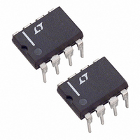
LTC1291CCN8 Linear Technology, LTC1291CCN8 Datasheet - Page 15

LTC1291CCN8
Manufacturer Part Number
LTC1291CCN8
Description
IC DATA ACQ SYSTEM 12BIT 8-DIP
Manufacturer
Linear Technology
Type
Data Acquisition System (DAS)r
Datasheet
1.LTC1291DCN8PBF.pdf
(20 pages)
Specifications of LTC1291CCN8
Resolution (bits)
12 b
Data Interface
Serial, Parallel
Voltage Supply Source
Single Supply
Voltage - Supply
5V
Operating Temperature
0°C ~ 70°C
Mounting Type
Through Hole
Package / Case
8-DIP (0.300", 7.62mm)
Lead Free Status / RoHS Status
Contains lead / RoHS non-compliant
Sampling Rate (per Second)
-
Available stocks
Company
Part Number
Manufacturer
Quantity
Price
Part Number:
LTC1291CCN8
Manufacturer:
LT
Quantity:
20 000
Company:
Part Number:
LTC1291CCN8#PBF
Manufacturer:
Linear Technology
Quantity:
135
A
Source Resistance
The analog inputs of the LTC1291 look like a 100pF
capacitor (C
gets switched between “+” and “–” inputs once during
each conversion cycle. Large external source resistors
or GND lead will cause gain errors and offset errors (Figure
7). For the best performance the LTC1291 should be
soldered directly to the PC board. If the source can not be
placed next to the pin and the gain parameter is important,
the pin should be Kelvin-sensed to eliminate parasitic
resistances due to long PC traces. For example, 0.1 of
resistance in the V
(I
When the input MUX is selected for single-ended input the
minus terminal is connected to GND internally on the die.
Any parasitic resistance from the GND pin to the ground
plane will lead to an offset voltage (I
CC
PPLICATI
V
V
Figure 7. Parasitic Resistance in the V
IN
IN
• 0.1 / V
+
–
R
P2
GND
R
R
SOURCE
SOURCE
Figure 8. Analog Input Equivalent Circuit
IN
CC
) in series with a 500 resistor (R
+
–
) of gain error for V
O
U
C1
INPUT
C2
CC
INPUT
“–”
“+”
S
–
+
lead can typically cause 0.5LSB
LTC1291
I FOR ATIO
U
D/A
5TH CLK
3RD CLK
REF
REF
+
–
CC
R
W
CC
ON
CC
= 5V.
= 500
• R
and GND Leads
V
P2
CC
LTC1291
C
100pF
).
IN
R
LTC1291 F08
LTC1291 F07
P1
=
U
ON
5V
). C
IN
and capacitances will slow the settling of the inputs. It is
important that the overall RC time constant is short
enough to allow the analog inputs to settle completely
within the allowed time.
“+” Input Settling
The input capacitor is switched onto the “+” input during
the sample phase (t
is 2.5 CLK cycles before a conversion starts. The voltage
on the “+” input must settle completely within the sample
period. Minimizing R
settling time. If large “+” input source resistance must be
used, the sample time can be increased by using a slower
CLK frequency. With the minimum possible sample time
of 2.5 s, R
adequate settle time.
“–” Input Settling
At the end of the sample phase the input capacitor switches
to the “–” input and the conversion starts (see Figure 9).
During the conversion, the “+” input voltage is effectively
“held” by the sample-and-hold and will not affect the
conversion result. It is critical that the “–” input voltage be
free of noise and settle completely during the first CLK
cycle of the conversion. Minimizing R
improve settling time. If large “–” input source resistance
must be used, the time can be extended by using a slower
CLK frequency. At the maximum CLK frequency of 1MHz,
R
settling.
Input Op Amps
When driving the analog inputs with an op amp, it is
important that the op amp settles within the allowed time
(see Figure 9). Again the “+” and “–” input sampling times
can be extended as described above to accommodate
slower op amps. Most op amps including the LT1006 and
LT1013 single supply op amps can be made to settle well
even with the minimum settling windows of 2.5 s (“+”
input) and 1 s (“–” input) that occurs at the maximum
clock rate of 1MHz. Figures 10 and 11 show examples
adequate and poor op amp settling.
SOURCE
– < 250 and C2 < 20pF will provide adequate
SOURCE
+ < 1.0k and C1 < 20pF will provide
SMPL
SOURCE
, see Figure 9). The sample period
+ and C1 will improve the
SOURCE
LTC1291
– and C2 will
15
1291fa


