604-00026 Parallax Inc, 604-00026 Datasheet - Page 7
604-00026
Manufacturer Part Number
604-00026
Description
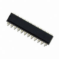
IC ADC 12BIT 8CH MAX1270 24-DIP
Manufacturer
Parallax Inc
Datasheet
1.604-00026.pdf
(20 pages)
Specifications of 604-00026
Number Of Bits
12
Sampling Rate (per Second)
110k
Data Interface
MICROWIRE™, QSPI™, Serial, SPI™
Number Of Converters
1
Power Dissipation (max)
1.07W
Voltage Supply Source
Single Supply
Operating Temperature
0°C ~ 70°C
Mounting Type
Through Hole
Package / Case
24-DIP
Lead Free Status / RoHS Status
Lead free / RoHS Compliant


(Typical Operating Circuit, V
110ksps; T
22, 24
13–20
3, 9,
DIP
2, 4
10
11
12
21
23
1
5
6
7
8
PIN
4, 7, 8,
11, 22,
24, 25,
15–21,
A
SSOP
2, 3
28
10
12
13
14
23
26
27
= +25°C; unless otherwise noted.)
1
5
6
9
8
7
6
5
4
3
2
1
0
0.1
CONVERSION RATE (USING STANDBY)
V
f
EXTERNAL CLOCK MODE.
LOW-RANGE UNIPOLAR MODE.
V
CLK
DD
CH_
____________________________________________________________________________________
AVERAGE SUPPLY CURRENT vs.
REFADJ
SSTRB
NAME
= 5V, INTERNAL REFERENCE,
= 2MHz
DGND
DOUT
SHDN
AGND
SCLK
CH0–
= 0
N.C.
CH7
V
REF
DIN
CS
DD
1
CONVERSION RATE (ksps)
DD
= +5V; external reference mode, V
+5V Supply. Bypass with a 0.1µF capacitor to AGND.
Digital Ground
No Connect. No internal connection.
Serial Clock Input. Clocks data in and out of serial interface. In external clock mode, SCLK also
sets the conversion speed.
Active-Low Chip-Select Input. Data is not clocked into DIN unless CS is low. When CS is high,
DOUT is high impedance.
Serial Data Input. Data is clocked in on the rising edge of SCLK.
Serial Strobe Output. In internal clock mode, SSTRB goes low after the falling edge of the eighth
SCLK and returns high when conversion is done. In external clock mode, SSTRB pulses high for one
clock period before the MSB decision. High impedance when CS is high in external clock mode.
Serial Data Output. Data is clocked out on the falling edge of SCLK. High impedance when CS is high.
Shutdown Input. When low, device is in FULLPD mode. Connect high for normal operation.
Analog Ground
Analog Input Channels
Bandgap Voltage-Reference Output/External Adjust Pin. Bypass with a 0.01µF capacitor to AGND.
Connect to V
Reference-Buffer Output/ADC Reference Input. In internal reference mode, the reference buffer pro-
vides a 4.096V nominal output, externally adjustable at REFADJ. In external reference mode, disable
the internal reference by pulling REFADJ to V
10
100
DD
when using an external reference at REF.
Typical Operating Characteristics (continued)
1000
Multirange, +5V, 8-Channel,
REF
= +4.096V; 4.7µF at REF; external clock, f
FUNCTION
DD
and applying the external reference to REF.
Serial 12-Bit ADCs
8
7
6
5
4
3
2
1
0
0.1
V
f
EXTERNAL CLOCK MODE.
LOW-RANGE UNIPOLAR MODE.
V
CLK
CONVERSION RATE (USING FULLPD)
DD
CH_
AVERAGE SUPPLY CURRENT vs.
= 5V, INTERNAL REFERENCE,
= 2MHz
= 0
1
CONVERSION RATE (ksps)
Pin Description
10
CLK
100
= 2MHz;
1000
7-175
Related parts for 604-00026
Image
Part Number
Description
Manufacturer
Datasheet
Request
R

Part Number:
Description:
IC EMBEDDED USB HOST 48-LQFP
Manufacturer:
Parallax Inc
Datasheet:

Part Number:
Description:
IC SENSOR TOUCH/PROXMTY 1CH 8DIP
Manufacturer:
Parallax Inc
Datasheet:


Part Number:
Description:
Microcontroller Modules & Accessories DISCONTINUED BY PARALLAX
Manufacturer:
Parallax Inc

Part Number:
Description:
BOOK UNDERSTANDING SIGNALS
Manufacturer:
Parallax Inc
Datasheet:


Part Number:
Description:
COMPETITION RING FOR SUMOBOT
Manufacturer:
Parallax Inc
Datasheet:


Part Number:
Description:
TEXT INFRARED REMOTE FOR BOE-BOT
Manufacturer:
Parallax Inc
Datasheet:
Part Number:
Description:
BOARD EXPERIMENT+LCD NX-1000
Manufacturer:
Parallax Inc
Datasheet:

Part Number:
Description:
CONTROLLER 16SERVO MOTOR CONTROL
Manufacturer:
Parallax Inc
Datasheet:

Part Number:
Description:
BASIC STAMP LOGIC ANALYZER
Manufacturer:
Parallax Inc
Datasheet: