AD7878SQ Analog Devices Inc, AD7878SQ Datasheet
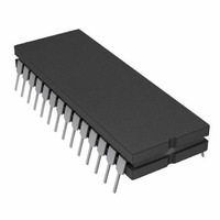
IC ADC 12BIT W/DSP INT 28-CDIP

AD7878SQ

Manufacturer Part Number
AD7878SQ
Description
IC ADC 12BIT W/DSP INT 28-CDIP
Manufacturer
Analog Devices Inc
Datasheet

Specifications of AD7878SQ

Rohs Status
RoHS non-compliant
Number Of Bits
12
Sampling Rate (per Second)
100k
Data Interface
DSP
Number Of Converters
1
Power Dissipation (max)
95.5mW
Voltage Supply Source
Analog and Digital, Dual ±
Operating Temperature
-55°C ~ 125°C
Mounting Type
Through Hole
Package / Case
28-CDIP (0.600", 15.24mm)

Available stocks

Company
Part Number
Manufacturer
Quantity
Price
Part Number:
AD7878SQ
Manufacturer:
NS
Quantity:
4
Part Number:
AD7878SQ
Manufacturer:
ADI/亚德诺
Quantity:
20 000
a
GENERAL DESCRIPTION
The AD7878 is a fast, complete, 12-bit A/D converter with a
versatile DSP interface consisting of an 8-word, first-in, first-out
(FIFO) memory and associated control logic.
The FIFO memory allows up to eight samples to be digitized
before the microprocessor is required to service the A/D con-
verter. The eight words can then be read out of the FIFO at
maximum microprocessor speed. A fast data access time of
41 ns allows direct interfacing to DSP processors and high
speed 16-bit microprocessors.
An on-chip status/control register allows the user to program the
effective length of the FIFO and contains the FIFO out of
range, FIFO empty and FIFO word count information.
The analog input of the AD7878 has a bipolar range of 3 V.
The AD7878 can convert full power signals up to 50 kHz and is
fully specified for dynamic parameters such as signal-to-noise
ratio and harmonic distortion.
The AD7878 is fabricated in Linear Compatible CMOS
(LC
bines precision bipolar circuits with low power CMOS logic.
The part is available in four package styles, 28-pin plastic and
hermetic dual-in-line package (DIP), leadless ceramic chip
carrier (LCCC) or plastic leaded chip carrier (PLCC).
REV. A
Information furnished by Analog Devices is believed to be accurate and
reliable. However, no responsibility is assumed by Analog Devices for its
use, nor for any infringements of patents or other rights of third parties
which may result from its use. No license is granted by implication or
otherwise under any patent or patent rights of Analog Devices.
FEATURES
Complete ADC with DSP Interface, Comprising:
72 dB SNR at 10 kHz Input Frequency
Interfaces to High Speed DSP Processors, e.g.,
41 ns max Data Access Time
Low Power, 60 mW typ
APPLICATIONS
Digital Signal Processing
Speech Recognition and Synthesis
Spectrum Analysis
High Speed Modems
DSP Servo Control
2
MOS), an advanced, mixed technology process that com-
Track/Hold Amplifier with 2 s Acquisition Time
7 s A/D Converter
3 V Zener Reference
8-Word FIFO and Interface Logic
ADSP-2100, TMS32010, TMS32020
100 kHz Sampling ADC with DSP Interface
One Technology Way, P.O. Box 9106, Norwood, MA 02062-9106, U.S.A.
Tel: 617/329-4700
Fax: 617/326-8703
PRODUCT HIGHLIGHTS
1. Complete A/D Function with DSP Interface
2. Dynamic Specifications for DSP Users
3. Fast Microprocessor Interface
The AD7878 provides the complete function for digitizing
ac signals to 12-bit accuracy. The part features an on-chip
track/hold, on-chip reference and 12-bit A/D converter. The
additional feature of an 8-word FIFO reduces the high soft-
ware overheads associated with servicing interrupts in DSP
processors.
The AD7878 is fully specified and tested for ac parameters,
including signal-to-noise ratio, harmonic distortion and
intermodulation distortion. Key digital timing parameters
are also tested and specified over the full operating tempera-
ture range.
Data access time of 41 ns is the fastest ever achieved in a
monolithic A/D converter, and makes the AD7878 compat-
ible with all modern 16-bit microprocessors and digital
signal processors.
FUNCTIONAL BLOCK DIAGRAM
LC
2
MOS Complete 12-Bit
World Wide Web Site: http://www.analog.com
© Analog Devices, Inc., 1997
AD7878

Related parts for AD7878SQ

AD7878SQ Summary of contents

Page 1

FEATURES Complete ADC with DSP Interface, Comprising: Track/Hold Amplifier with 2 s Acquisition Time 7 s A/D Converter 3 V Zener Reference 8-Word FIFO and Interface Logic 72 dB SNR at 10 kHz Input Frequency Interfaces to High Speed ...

Page 2

AD7878–SPECIFICATIONS Parameter 2 DYNAMIC PERFORMANCE 3 Signal-to-Noise Ratio (SNR MIN MAX Total Harmonic Distortion (THD) Peak Harmonic or Spurious Noise Intermodulation Distortion (IMD) Second Order Terms Third Order Terms Track/Hold Acquisition Time DC ACCURACY ...

Page 3

TIMING CHARACTERISTICS Limit Limit at T MIN MAX Parameter (L Grade) ( Grades CLK IN Cycles 2 CLK IN Cycles ...

Page 4

AD7878 Pin Pin Number Mnemonic Function 11 ADD0 Address Input. This control input determines whether the word placed on the output data bus during a read operation is a data word from the FIFO RAM or the contents of the ...

Page 5

... ORDERING GUIDE Signal- Temperature to-Noise 1, 2 Model Range Ratio AD7878JN + AD7878AQ – + AD7878SQ – +125 AD7878KN + AD7878BQ – + AD7878LN + AD7878SE – +125 AD7878JP + AD7878KP + AD7878LP + NOTES 1 To order MIL-STD-883, Class B processed parts, add /883B to part number. Contact our local sales office for military data sheet. ...

Page 6

AD7878 INTERNAL FIFO MEMORY The internal FIFO memory of the AD7878 consists of eight memory locations. Each word in memory contains 13 bits of information—12 bits of data from the conversion result and one additional bit which contains information as ...

Page 7

CLK IN cycles. Therefore, if read or write operations can occur during t periods, it means that the conversion time for ...

Page 8

AD7878 Extended Read/Write Operation As described earlier, a read/write operation to the AD7878 can cause spurious on-chip transients. Should these transients occur while the track/hold is going from track to hold mode, it may result in an incorrect value of ...

Page 9

Figure 11 shows a typical plot of effective number of bits versus frequency for an AD7878KN with a sampling frequency of 100 kHz. The effective number of bits typically falls between 11.7 and 11.85 corresponding to SNR figures of 72.2 ...

Page 10

AD7878 CONVERSION TIMING The track-and-hold on the AD7878 goes from track-to-hold mode on the rising edge of CONVST, and the value of V this point is the value which will be converted. However, the conversion actually sorts on the next ...

Page 11

Positive Full-Scale Adjust Apply a voltage of 2.9978 V (FS/2 – 3/2 LSBs until the ADC output code flickers between 0111 1111 1110 and 0111 1111 1111. Negative Full-Scale Adjust Apply a voltage of –2.9993 V (–FS/2 + ...

Page 12

AD7878 The MC68000 AS and R/W outputs are used to generate sepa- rate DMWR and DMRD inputs for the AD7878. As with the three interfaces previously described, WAIT states are inserted if a read/write operation is attempted while the track/hold ...

Page 13

Establish a single point analog ground (star ground) separate from the logic system ground at Pin 22 (AGND dose as possible to the AD7878, as shown in Figure 22. Connect all other grounds and Pin 7 (AD7878 DGND) ...

Page 14

AD7878 Figure 23. Data Acquisition Circuit Using the AD7878 Figure 24. PCB Silkscreen for Figure 23 –14– REV. A ...

Page 15

Figure 25. PCB Component Side Layout for Figure 23 REV. A Figure 26. PCB Solder Side Layout for Figure 23 –15– AD7878 ...

Page 16

AD7878 Table IV. TMS32010/TMS32020 Interface Connections IDC Signal Connect TMS32010 Contact No. Mnemonic Signal 1 R/W — STRB 2 — DMRD DEN 3 DMWR READY — RESET RESET 7 ALFL INT 8 9 ADD0 ...

Related keywords