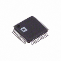
AD9226ASTRL Analog Devices Inc, AD9226ASTRL Datasheet - Page 6

AD9226ASTRL
Manufacturer Part Number
AD9226ASTRL
Description
IC ADC 12BIT 65MSPS 48-LQFP
Manufacturer
Analog Devices Inc
Datasheet
1.AD9226ASTZ.pdf
(28 pages)
Specifications of AD9226ASTRL
Rohs Status
RoHS non-compliant
Number Of Bits
12
Sampling Rate (per Second)
65M
Data Interface
Parallel
Number Of Converters
3
Power Dissipation (max)
475mW
Voltage Supply Source
Single Supply
Operating Temperature
-40°C ~ 85°C
Mounting Type
Surface Mount
Package / Case
48-LQFP
For Use With
AD9226-EB - BOARD EVAL FOR AD9226-SSOP
Available stocks
Company
Part Number
Manufacturer
Quantity
Price
Company:
Part Number:
AD9226ASTRL
Manufacturer:
Analog Devices Inc
Quantity:
10 000
AD9226
Pin
Number
1, 2, 32, 33 AVSS
3, 4, 31, 34 AVDD
5, 6, 8, 10, NC
11, 44
7
9
12
13
14, 22, 30
15, 23, 29
16–21,
24–26
27
28
35
36
37
38
39, 40
41, 42
43
45
46
47
48
NC = NO CONNECT
(LSB) BIT 12
AVDD
AVDD
AVSS
AVSS
OEB
CLK
NC
NC
NC
NC
NC
48-PIN FUNCTION DESCRIPTIONS
Name
CLK
OEB
BIT 12
BIT 11
DRVSS
DRVDD
BITS 10–5,
BITS 4–2
BIT 1
OTR
MODE2
SENSE
VREF
REFCOM
(AVSS)
CAPB
CAPT
MODE1
CM LEVEL
VINA
VINB
VR
10
11
12
1
2
3
4
5
6
7
8
9
48 47 46 45 44
13 14 15 16 17 18 19 20 21 22 23 24
PIN 1
IDENTIFIER
PIN CONNECTION
48-Lead LQFP
(Not to Scale)
TOP VIEW
AD9226
Description
Analog Ground
5 V Analog Supply
Clock Input Pin
Output Enable (Active Low)
Digital Output Driver Ground
3 V to 5 V Digital Output
Out of Range
Data Format Select
Reference Select
Reference In/Out
Reference Common
Noise Reduction Pin
Noise Reduction Pin
Clock Stabilizer
Analog Input Pin (+)
Analog Input Pin (–)
Noise Reduction Pin
43 42 41 40
No Connect
Least Significant Data Bit (LSB)
Data Output Bit
Driver Supply
Data Output Bits
Most Significant Data Bit (MSB)
Midsupply Reference
39 38 37
36
35
34
33
32
31
30
29
28
26
25
27
SENSE
MODE2
AVDD
AVSS
AVSS
AVDD
DRVSS
DRVDD
OTR
BIT 1 (MSB)
BIT 2
BIT 3
Pin
Number
1
2
3–12
13
14
15, 26
16, 25
17
18
19
20
21
22
23
24
27
28
28-PIN FUNCTION DESCRIPTIONS
Name
CLK
BIT 12
BITS 11–2
BIT 1
OTR
AVDD
AVSS
SENSE
VREF
REFCOM
(AVSS)
CAPB
CAPT
MODE
VINA
VINB
DRVSS
DRVDD
(LSB) BIT 12
(MSB) BIT 1
BIT 11
BIT 10
BIT 9
BIT 8
BIT 7
BIT 6
BIT 5
BIT 4
BIT 3
BIT 2
OTR
CLK
PIN CONNECTION
28-Lead SSOP
10
11
12
13
14
1
2
3
4
5
6
7
8
9
Description
Clock Input Pin
Least Significant Data Bit (LSB)
Data Output Bits
Most Significant Data Bit (MSB)
Out of Range
5 V Analog Supply
Analog Ground
Reference Select
Input Span Select (Reference I/O)
Reference Common
Noise Reduction Pin
Noise Reduction Pin
Data Format Select /Clock Stabilizer
Analog Input Pin (+)
Analog Input Pin (–)
Digital Output Driver Ground
3 V to 5 V Digital Output
Driver Supply
(Not to Scale)
TOP VIEW
AD9226
28
27
26
25
24
23
22
21
20
19
18
17
16
15
DRVDD
DRVSS
AVDD
AVSS
VINB
VINA
MODE
CAPT
CAPB
REFCOM (AVSS)
VREF
SENSE
AVSS
AVDD


