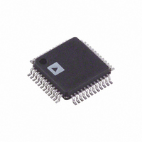
AD9226ASTRL Analog Devices Inc, AD9226ASTRL Datasheet - Page 3

AD9226ASTRL
Manufacturer Part Number
AD9226ASTRL
Description
IC ADC 12BIT 65MSPS 48-LQFP
Manufacturer
Analog Devices Inc
Datasheet
1.AD9226ASTZ.pdf
(28 pages)
Specifications of AD9226ASTRL
Rohs Status
RoHS non-compliant
Number Of Bits
12
Sampling Rate (per Second)
65M
Data Interface
Parallel
Number Of Converters
3
Power Dissipation (max)
475mW
Voltage Supply Source
Single Supply
Operating Temperature
-40°C ~ 85°C
Mounting Type
Surface Mount
Package / Case
48-LQFP
For Use With
AD9226-EB - BOARD EVAL FOR AD9226-SSOP
Available stocks
Company
Part Number
Manufacturer
Quantity
Price
Company:
Part Number:
AD9226ASTRL
Manufacturer:
Analog Devices Inc
Quantity:
10 000
DIGITAL SPECIFICATIONS
Parameters
LOGIC INPUTS (Clock, DFS
Output Enable
LOGIC OUTPUTS (With DRVDD = 5 V)
LOGIC OUTPUTS (With DRVDD = 3 V)
NOTES
1
Specifications subject to change without notice.
SWITCHING SPECIFICATIONS
Parameters
Max Conversion Rate
Clock Period
CLOCK Pulsewidth High
CLOCK Pulsewidth Low
Output Delay
Pipeline Delay (Latency)
Output Enable Delay
NOTES
1
2
3
Specifications subject to change without notice.
LQFP package.
The clock period may be extended to 10 µs without degradation in specified performance @ 25°C.
When MODE pin is tied to AVDD or grounded, the AD9226 SSOP is not affected by clock duty cycle.
LQFP package.
High-Level Input Voltage
Low-Level Input Voltage
High-Level Input Current (V
Low-Level Input Current (V
Input Capacitance
Output Enable
High-Level Output Voltage (I
High-Level Output Voltage (I
Low-Level Output Voltage (I
Low-Level Output Voltage (I
Output Capacitance
High-Level Output Voltage (I
High-Level Output Voltage (I
Low-Level Output Voltage (I
Low-Level Output Voltage (I
1
1
)
1
3
2
2
ANALOG
CLOCK
IN
1
IN
OL
OL
OL
OL
INPUT
DATA
, Duty Cycle
OH
OH
OH
OH
OUT
= 0 V)
= AVDD)
= 1.6 mA)
= 50 µA)
= 1.6 mA)
= 50 µA)
= 50 µA)
= 0.5 mA)
= 50 µA)
= 0.5 mA)
(AVDD = 5 V, DRVDD = 3 V, f
n
n–8
1
(T
n+1
, and
n–7
MIN
to T
n+2
n–6
Temp
Full
Full
Full
Full
Full
MAX
Full
Full
Full
Full
Full
Full
Full
Full
Full
Temp
Full
Full
Full
Full
Full
Full
Full
with AVDD = 5 V, DRVDD = 3 V, C
n+3
n–5
V
IV
IV
IV
IV
IV
IV
IV
IV
Test Level
IV
IV
IV
IV
IV
n+4
n–4
SAMPLE
Test Level
VI
V
V
V
V
V
V
= 65 MSPS, VREF = 2.0 V, T
n+5
n–3
DRVDD
n+6
Min
2.4
–10
–10
4.5
2.4
2.95
2.80
n–2
2
n+7
n–1
Min
65
15.38
3
3
3.5
L
– .
= 20 pF)
0 5
n+8
TOD = 7.0 MAX
n
Typ
5
5
3.5 MIN
MIN
n+1
Typ
7
15
to T
MAX
Max
0.8
+10
+10
DRVDD
0.4
0.1
0.4
0.05
, unless otherwise noted.)
2
Max
7
+ .
0 5
Clock Cycles
Unit
MHz
ns
ns
ns
ns
ns
AD9226
Unit
V
V
µA
µA
pF
V
V
V
V
V
pF
V
V
V
V


