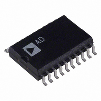
AD7701AR Analog Devices Inc, AD7701AR Datasheet - Page 5

AD7701AR
Manufacturer Part Number
AD7701AR
Description
IC ADC 16BIT LC2MOS 20-SOIC
Manufacturer
Analog Devices Inc
Datasheet
1.AD7701ARZ.pdf
(20 pages)
Specifications of AD7701AR
Rohs Status
RoHS non-compliant
Number Of Bits
16
Sampling Rate (per Second)
4k
Data Interface
Serial
Number Of Converters
1
Power Dissipation (max)
37mW
Voltage Supply Source
Analog and Digital, Dual ±
Operating Temperature
-40°C ~ 85°C
Mounting Type
Surface Mount
Package / Case
20-SOIC (0.300", 7.50mm Width)
Available stocks
Company
Part Number
Manufacturer
Quantity
Price
Company:
Part Number:
AD7701AR
Manufacturer:
ADI
Quantity:
2 197
Part Number:
AD7701AR
Manufacturer:
ADI/亚德诺
Quantity:
20 000
Part Number:
AD7701ARS
Manufacturer:
ADI/亚德诺
Quantity:
20 000
Company:
Part Number:
AD7701ARSZ
Manufacturer:
MICROCHIP
Quantity:
1 000
Part Number:
AD7701ARZ
Manufacturer:
ADI/亚德诺
Quantity:
20 000
PDIP,
CERDIP,
SOIC
1
2
3
4, 17
5
6
7
8
9
10
11
12
13
14
15
16
18
19
20
REV. E
Pin No.
SSOP
1
2
3
4, 25
5
8
6, 7, 9, 11,
18, 21, 22, 23
10
12
13
14
15
16
17
19
20
24
26
27
28
Mnemonic Description
MODE
CLKOUT
CLKIN
SC1, SC2
DGND
DV
NC
AV
AGND
A
V
SLEEP
BP/UP
CAL
AV
DV
CS
DRDY
SCLK
SDATA
IN
REF
SS
DD
SS
DD
Selects the Serial Interface Mode. If MODE is tied to –5 V, the AD7701 will operate in
the Asynchronous Communications (AC) mode. The SCLK pin is configured as an
input, and data is transmitted in two bytes, each with one start bit and two stop bits. If
MODE is tied to DGND, the Synchronous External Clocking (SEC) mode is selected.
SCLK is configured as an input, and the output appears without formatting, the MSB
coming first. If MODE is tied to +5 V, the AD7701 operates in the Synchronous
Self-Clocking (SSC) mode. SCLK is configured as an output, with a clock frequency of
f
Clock Output to Generate an Internal Master Clock by Connecting a Crystal between
CLKOUT and CLKIN. If an external clock is used, CLKOUT is not connected.
Clock Input for External Clock.
System Calibration Pins. The state of these pins, when CAL is taken high, determines
the type of calibration performed.
Digital Ground. Ground reference for all digital signals.
Digital Negative Supply, –5 V Nominal.
No Connect.
Analog Negative Supply, –5 V Nominal.
Analog Ground. Ground reference for all analog signals.
Analog Input.
Voltage Reference Input, 2.5 V Nominal. This determines the value of positive full scale
in the Unipolar mode and of both positive and negative full scale in Bipolar mode.
Sleep Mode Pin. When this pin is taken low, the AD7701 goes into a low power mode
with typically 10 µW power consumption.
Bipolar/Unipolar Mode Pin. When this pin is low, the AD7701 is configured for a uni-
polar input range going from AGND to V
configured for a bipolar input range, ± V
Calibration Mode Pin. When CAL is taken high for more than four cycles, the AD7701
is reset and performs a calibration cycle when CAL is brought low again. The CAL pin
can also be used as a strobe to synchronize the operation of several AD7701s.
Analog Positive Supply, +5 V Nominal.
Digital Positive Supply, +5 V Nominal.
Chip Select Input. When CS is brought low, the AD7701 will begin to transmit serial
data in a format determined by the state of the MODE pin.
Data Ready Output. DRDY is low when valid data is available in the output register. It
goes high after transmission of a word is completed. It also goes high for four clock
cycles when a new data-word is being loaded into the output register, to indicate that
valid data is not available, irrespective of whether data transmission is complete or not.
Serial Clock Input/Output. The SCLK pin is configured as an input or output, depen-
dent on the type of serial data transmission that has been selected by the MODE pin.
When configured as an output in the Synchronous Self-Clocking mode, it has a fre-
quency of f
Serial Data Output. The AD7701’s output data is available at this pin as a 16-bit serial
word. The transmission format is determined by the state of the MODE pin.
CLKlN
PIN FUNCTION DESCRIPTIONS
/4 and 25% duty cycle.
CLKIN
/4 and a duty cycle of 25%.
–5–
REF
.
REF
. When Pin 12 is high, the AD7701 is
AD7701


