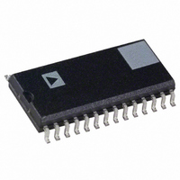
AD9225AR Analog Devices Inc, AD9225AR Datasheet - Page 11

AD9225AR
Manufacturer Part Number
AD9225AR
Description
IC ADC 12BIT 25MSPS 28-SOIC
Manufacturer
Analog Devices Inc
Datasheet
1.AD9225ARZ.pdf
(25 pages)
Specifications of AD9225AR
Mounting Type
Surface Mount
Rohs Status
RoHS non-compliant
Number Of Bits
12
Sampling Rate (per Second)
25M
Data Interface
Parallel
Number Of Converters
7
Power Dissipation (max)
373mW
Voltage Supply Source
Single Supply
Operating Temperature
-40°C ~ 85°C
Package / Case
28-SOIC (0.300", 7.50mm Width)
Power Dissipation Pd
383mW
Input Channels Per Adc
1
No. Of Channels
1
Peak Reflow Compatible (260 C)
No
Sample Rate
25MSPS
Supply Voltage Max
5V
No. Of Bits
12 Bit
For Use With
AD9225-EB - BOARD EVAL FOR AD9225
Lead Free Status / RoHS Status
Contains lead / RoHS non-compliant
Available stocks
Company
Part Number
Manufacturer
Quantity
Price
Part Number:
AD9225AR
Manufacturer:
ADI/亚德诺
Quantity:
20 000
Company:
Part Number:
AD9225ARS
Manufacturer:
ADI
Quantity:
288
Part Number:
AD9225ARS
Manufacturer:
ADI/亚德诺
Quantity:
20 000
Part Number:
AD9225ARSRL
Manufacturer:
ADI/亚德诺
Quantity:
20 000
Company:
Part Number:
AD9225ARSZ
Manufacturer:
ADI
Quantity:
1 000
Part Number:
AD9225ARSZ
Manufacturer:
ADI/亚德诺
Quantity:
20 000
Company:
Part Number:
AD9225ARSZRL
Manufacturer:
ADI
Quantity:
1 000
Part Number:
AD9225ARZ
Manufacturer:
ADI/亚德诺
Quantity:
20 000
Rev. C
Input
Connection
Single-Ended
Single-Ended
Differential
(via Transformer)
or Amplifier
*VINA and VINB can be interchanged if signal inversion is required.
Reference
Operating Mode
Internal
Internal
Internal
External
(Nondynamic)
External
(Dynamic)
Coupling Span (V) VINA*
DC
AC
AC/DC
Input Span (VINA–VINB)
(V p-p)
2
4
2 £ SPAN £ 4 and
SPAN = 2
2 £ SPAN £ 4
2 £ SPAN £ 4
Input
2
2 ¥ VREF 0 to
4
2 ¥ VREF 2.0 – VREF
2 or
2 ¥ VREF 0 to 2 ¥ VREF
4
2 ¥ VREF 2.0 – VREF
2
2 ¥ VREF 2.0 – VREF/2
4.0
VREF
Table I. Analog Input Configuration Summary
Table II. Reference Configuration Summary
0 to 2
2 ¥ VREF
0 to 4
to
2.0 + VREF
0 to 1 or
0.5 to 4.5
to
2.0 + VREF
2 to 3
to
2.0 + VREF/2
1.5 to 3.5
Input Range (V)
Required VREF (V)
1
2
1 £ VREF £ 2.0 and
VREF = (1 + R1/R2)
1 £ VREF £ 2.0
CAPT and CAPB
Externally Driven
1
1 or VREF
3 to 2
VINB*
VREF
2.0
2.0
2.0
2.0
2.0 + VREF/2 12, 13
to
2.0 – VREF/2
3.5 to 1.5
–11–
Figure
No.
8, 9
8, 9
8, 9
21
10, 11
11
10
12, 13
12, 13
Connect
SENSE
SENSE
R1
R2
SENSE
VREF
SENSE
VREF
External Reference
External Reference
Comments
Best for stepped input response applications;
requires ± 5 V op amp.
Same as above but with improved noise
performance due to increase in dynamic
range. Headroom/settling time requirements
of ± 5 V op amp should be evaluated.
Optimum noise performance, excellent THD
performance, often requires low distortion op
amp with VCC > +5 V due to its headroom
issues.
Optimum THD performance with VREF = 1.
Single-supply operation (i.e., +5 V) for many
op amps.
Optimum noise performance, excellent THD
performance; ability to use ± 5 V op amp.
Flexible input range, optimum THD perfor-
mance with VREF = 1. Ability to use either
+5 V or ± 5 V op amp.
Optimum full-scale THD and SFDR perfor-
mance well beyond the ADC’s Nyquist
frequency. Preferred mode for under-
sampling applications.
Same as above with the exception that full-
scale THD and SFDR performance can be
traded off for better noise performance.
Optimum noise performance.
External Reference
To
VREF
REFCOM
VREF and SENSE
SENSE and REFCOM
AVDD
AVDD
AVSS
CAPT
CAPB
AD9225


