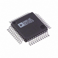
AD7864ASZ-2 Analog Devices Inc, AD7864ASZ-2 Datasheet - Page 8

AD7864ASZ-2
Manufacturer Part Number
AD7864ASZ-2
Description
IC ADC 14BIT DUAL 4CHAN 44-MQFP
Manufacturer
Analog Devices Inc
Datasheet
1.AD7864ASZ-1.pdf
(28 pages)
Specifications of AD7864ASZ-2
Data Interface
Parallel
Number Of Bits
12
Sampling Rate (per Second)
520k
Number Of Converters
1
Power Dissipation (max)
120mW
Voltage Supply Source
Analog and Digital
Operating Temperature
-40°C ~ 85°C
Mounting Type
Surface Mount
Package / Case
44-MQFP, 44-PQFP
Resolution (bits)
12bit
Sampling Rate
500kSPS
Input Channel Type
Single Ended
Supply Voltage Range - Analog
4.75V To 5.25V
Supply Current
24mA
Digital Ic Case Style
QFP
Number Of Elements
1
Resolution
12Bit
Architecture
SAR
Sample Rate
520KSPS
Input Polarity
Unipolar
Input Type
Voltage
Rated Input Volt
2.5/5V
Differential Input
No
Power Supply Requirement
Analog and Digital
Single Supply Voltage (typ)
5V
Single Supply Voltage (min)
4.75V
Single Supply Voltage (max)
5.25V
Dual Supply Voltage (typ)
Not RequiredV
Dual Supply Voltage (min)
Not RequiredV
Dual Supply Voltage (max)
Not RequiredV
Power Dissipation
120mW
Differential Linearity Error
±0.9LSB
Integral Nonlinearity Error
±1LSB
Operating Temp Range
-40C to 85C
Operating Temperature Classification
Industrial
Mounting
Surface Mount
Pin Count
44
Package Type
MQFP
Input Signal Type
Single-Ended
Lead Free Status / RoHS Status
Lead free / RoHS Compliant
Lead Free Status / RoHS Status
Lead free / RoHS Compliant, Lead free / RoHS Compliant
Available stocks
Company
Part Number
Manufacturer
Quantity
Price
Company:
Part Number:
AD7864ASZ-2
Manufacturer:
Analog Devices Inc
Quantity:
135
Company:
Part Number:
AD7864ASZ-2
Manufacturer:
Analog Devices Inc
Quantity:
10 000
Part Number:
AD7864ASZ-2
Manufacturer:
ADI/亚德诺
Quantity:
20 000
Company:
Part Number:
AD7864ASZ-2REEL
Manufacturer:
Analog Devices Inc
Quantity:
10 000
AD7864
Pin No.
27
28
29 to 34
35
36
37
38, 39
40 to 43
44
Mnemonic
INT /EXT CLK
CLKIN
DB11 to DB6
DV
V
DGND
DB5, DB4
DB3 to DB0
EOC
DRIVE
DD
Description
Internal/External Clock Select Input. When this pin is at Logic 0, the AD7864 uses its internally generated master
clock. When this pin is at Logic 1, the master clock is generated externally to the device.
Conversion Clock Input. This is an externally applied clock that allows the user to control the conversion rate of
the AD7864. Each conversion needs 14 clock cycles for the conversion to be completed and an EOC pulse to be
generated. The clock should have a duty cycle that is no worse than 60/40. See the
section.
Data Bit 11 is the MSB, followed by Data Bit 10 to Data Bit 6. Three-state TTL outputs. Output coding is twos
complement for the AD7864-1 and AD7864-3. Output coding is straight (natural) binary for the AD7864-2.
Positive Supply Voltage for Digital Section, 5.0 V ± 5%. Connect a 0.1 μF decoupling capacitor between this pin
and AGND. Both DV
This pin provides the positive supply voltage for the output drivers (DB0 to DB11), BUSY, EOC , and FRSTDATA. It
is normally tied to DV
the conversion sequence. To facilitate interfacing to 3 V processors and DSPs, the output data drivers can also be
powered by a 3 V ± 10% supply.
Digital Ground. This is the ground reference for digital circuitry. Connect this DGND pin to the AGND plane of
the system at the AGND pin.
Data Bit 5 to Data Bit 4. Three-state TTL outputs.
Data Bit 3 to Data Bit 0. Bidirectional data pins. When a read operation takes place, these pins are three-state TTL
outputs. The channel select register is programmed with the data on the DB0 to DB3 pins with standard CS and
WR signals. DB0 represents Channel 1, and DB3 represents Channel 4.
End-of-Conversion. Active low logic output indicating conversion status. The end of each conversion in a
conversion sequence is indicated by a low-going pulse on this line.
DD
DD
and AV
. Decouple V
DD
should be externally tied together.
Rev. D | Page 8 of 28
DRIVE
with a 0.1 μF capacitor to improve performance when reading during
Using An External Clock


