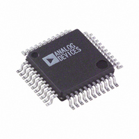
AD7864ASZ-2 Analog Devices Inc, AD7864ASZ-2 Datasheet - Page 13

AD7864ASZ-2
Manufacturer Part Number
AD7864ASZ-2
Description
IC ADC 14BIT DUAL 4CHAN 44-MQFP
Manufacturer
Analog Devices Inc
Datasheet
1.AD7864ASZ-1.pdf
(28 pages)
Specifications of AD7864ASZ-2
Data Interface
Parallel
Number Of Bits
12
Sampling Rate (per Second)
520k
Number Of Converters
1
Power Dissipation (max)
120mW
Voltage Supply Source
Analog and Digital
Operating Temperature
-40°C ~ 85°C
Mounting Type
Surface Mount
Package / Case
44-MQFP, 44-PQFP
Resolution (bits)
12bit
Sampling Rate
500kSPS
Input Channel Type
Single Ended
Supply Voltage Range - Analog
4.75V To 5.25V
Supply Current
24mA
Digital Ic Case Style
QFP
Number Of Elements
1
Resolution
12Bit
Architecture
SAR
Sample Rate
520KSPS
Input Polarity
Unipolar
Input Type
Voltage
Rated Input Volt
2.5/5V
Differential Input
No
Power Supply Requirement
Analog and Digital
Single Supply Voltage (typ)
5V
Single Supply Voltage (min)
4.75V
Single Supply Voltage (max)
5.25V
Dual Supply Voltage (typ)
Not RequiredV
Dual Supply Voltage (min)
Not RequiredV
Dual Supply Voltage (max)
Not RequiredV
Power Dissipation
120mW
Differential Linearity Error
±0.9LSB
Integral Nonlinearity Error
±1LSB
Operating Temp Range
-40C to 85C
Operating Temperature Classification
Industrial
Mounting
Surface Mount
Pin Count
44
Package Type
MQFP
Input Signal Type
Single-Ended
Lead Free Status / RoHS Status
Lead free / RoHS Compliant
Lead Free Status / RoHS Status
Lead free / RoHS Compliant, Lead free / RoHS Compliant
Available stocks
Company
Part Number
Manufacturer
Quantity
Price
Company:
Part Number:
AD7864ASZ-2
Manufacturer:
Analog Devices Inc
Quantity:
135
Company:
Part Number:
AD7864ASZ-2
Manufacturer:
Analog Devices Inc
Quantity:
10 000
Part Number:
AD7864ASZ-2
Manufacturer:
ADI/亚德诺
Quantity:
20 000
Company:
Part Number:
AD7864ASZ-2REEL
Manufacturer:
Analog Devices Inc
Quantity:
10 000
CIRCUIT DESCRIPTION
ANALOG INPUT
The AD7864 is offered in three models: the AD7864-1, where
each input can be configured for ±10 V or a ±5 V input voltage
range; the AD7864-3, which handles the input voltage range of
±2.5 V; and the AD7864-2, where each input can be configured
to have a 0 V to +2.5 V or 0 V to +5 V input voltage range.
AD7864-1
Figure 4 shows the analog input section of the AD7864-1. Each
input can be configured for ±5 V or ±10 V operation on the
AD7864-1. For ±5 V (AD7864-1) operation, the V
inputs are tied together and the input voltage is applied to both.
For ±10 V (AD7864-1) operation, the V
and the input voltage is applied to the V
V
ease of printed circuit board (PCB) layout on the ±10 V range,
the input voltage may be applied to the V
V
For the AD7864-1, R1 = 6 kΩ, R2 = 24 kΩ, R3 = 24 kΩ, and
R4 = 12 kΩ. The resistor input stage is followed by the high
input impedance stage of the track-and-hold amplifier.
The designed code transitions take place midway between
successive integer least significant bit values (that is, 1/2 LSB,
3/2 LSB, 5/2 LSB, and so forth). Least significant bit size is given
by the formula 1 LSB = FSR/4096. For the ±5 V range, 1 LSB =
10 V/4096 = 2.44 mV. For the ±10 V range, 1 LSB = 20 V/4096 =
4.88 mV. Output coding is twos complement binary with 1 LSB =
FSR/4096. The ideal input/output transfer function for the
AD7864-1 is shown in Table 5.
INxB
INxA
V
V
V
IN1A
IN1B
REF
inputs are symmetrical and fully interchangeable. Thus for
input is tied to AGND.
Figure 4. AD7864-1 Analog Input Structure
R2
R3
6kΩ
AGND
R1
R4
REFERENCE
TO ADC
REFERENCE
CIRCUITRY
T/H
INxB
2.5V
INxA
INxB
input is tied to AGND
input. The V
input while the
TO INTERNAL
COMPARATOR
AD7864-1
INxA
and V
INxA
INxB
and
Rev. D | Page 13 of 28
Table 5. Ideal Input/Output Code Table for the AD7864-1
Analog Input
+FSR/2 − 3/2 LSB
+FSR/2 − 5/2 LSB
+FSR/2 − 7/2 LSB
AGND + 3/2 LSB
AGND + 1/2 LSB
AGND − 1/2 LSB
AGND − 3/2 LSB
−FSR/2 + 5/2 LSB
−FSR/2 + 3/2 LSB
−FSR/2 + 1/2 LSB
1
2
AD7864-2
Figure 5 shows the analog input section of the AD7864-2. Each
input can be configured for 0 V to 5 V operation or 0 V to 2.5 V
operation. For 0 V to 5 V operation, the V
AGND and the input voltage is applied to the V
0 V to 2.5 V operation, the V
and the input voltage is applied to both. The V
inputs are symmetrical and fully interchangeable. Thus for ease
of PCB layout on the 0 V to 5 V range, the input voltage may be
applied to the V
For the AD7864-2, R1 = 6 kΩ and R2 = 6 kΩ. The designed
code transitions occur on successive integer least significant bit
values. Output coding is straight (natural) binary with 1 LSB =
FSR/4096 = 2.5 V/4096 = 0.61 mV, and 5 V/4096 = 1.22 mV, for
the 0 V to 2.5 V and 0 V to 5 V options, respectively.
Table 6 shows the ideal input and output transfer function for
the AD7864-2.
FSR is full-scale range and is 20 V for the ±10 V range and +10 V for the ±5 V
range, with V
1 LSB = FSR/4096 = 4.883 mV (±10 V for the AD7864-1) and 2.441 mV (±5 V
for the AD7864-1) with V
V
V
V
IN1A
IN1B
REF
REF
1
= 2.5 V.
R2
Figure 5. AD7864-2 Analog Input Structure
R1
INxB
2
input while the V
REF
6kΩ
= 2.5 V.
Digital Output Code Transition
011...110 to 011...111
011...101 to 011...110
011...100 to 011...101
000...001 to 000...010
000...000 to 000...001
111...111 to 000...000
111...110 to 111...111
100...010 to 100...011
100...001 to 100...010
100...000 to 100...001
INxA
and V
REFERENCE
TO ADC
REFERENCE
CIRCUITRY
INxB
INxA
T/H
2.5V
inputs are tied together
input is tied to AGND.
INxB
input is tied to
AD7864-2
INxA
TO INTERNAL
COMPARATOR
INxA
and V
input. For
AD7864
INxB


