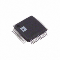
AD7484BSTZ Analog Devices Inc, AD7484BSTZ Datasheet - Page 14

AD7484BSTZ
Manufacturer Part Number
AD7484BSTZ
Description
IC ADC 14BIT SAR 3MSPS 48-LQFP
Manufacturer
Analog Devices Inc
Datasheet
1.AD7484BSTZ.pdf
(20 pages)
Specifications of AD7484BSTZ
Data Interface
Parallel
Number Of Bits
14
Sampling Rate (per Second)
3M
Number Of Converters
1
Power Dissipation (max)
90mW
Voltage Supply Source
Analog and Digital
Operating Temperature
-40°C ~ 85°C
Mounting Type
Surface Mount
Package / Case
48-LQFP
Resolution (bits)
14bit
Sampling Rate
3MSPS
Input Channel Type
Single Ended
Supply Voltage Range - Analog
4.75V To 5.25V
Supply Voltage Range - Digital
4.75V To 5.25V
Lead Free Status / RoHS Status
Lead free / RoHS Compliant
For Use With
EVAL-AD7484CBZ - BOARD EVALUATION FOR AD7484
Lead Free Status / RoHS Status
Lead free / RoHS Compliant, Lead free / RoHS Compliant
Available stocks
Company
Part Number
Manufacturer
Quantity
Price
Company:
Part Number:
AD7484BSTZ
Manufacturer:
ADI30
Quantity:
221
Company:
Part Number:
AD7484BSTZ
Manufacturer:
Analog Devices Inc
Quantity:
10 000
Part Number:
AD7484BSTZ
Manufacturer:
ADI/亚德诺
Quantity:
20 000
AD7484
Figure 18 shows the AD7484 conversion sequence if the part
was put into NAP mode after each conversion.
Figure 19 and Figure 20 show a typical graphical representation
of power versus throughput for the AD7484 when in normal
and NAP modes, respectively.
In standby mode, all internal circuitry is powered down and the
power consumption of the AD7484 is reduced to 10 µW. The
power-up time necessary before a conversion can be initiated is
longer because more of the internal circuitry has been powered
down. In using the internal reference of the AD7484, the ADC
must be brought out of standby mode 500 ms before a
CONVST
BUSY
NAP
90
85
80
75
70
65
60
90
80
70
60
50
40
30
20
10
0
0
0
Figure 19. Normal Mode, Power vs. Throughput
250
300ns
Figure 20. NAP Mode, Power vs. Throughput
500
Figure 18. NAP Mode Power Dissipation
600ns
500
1000
THROUGHPUT (kSPS)
THROUGHPUT (kSPS)
750
1500
1000
2µs
1400ns
1250
2000
1500
2500
1750
2000
3000
Rev. A | Page 14 of 20
conversion is initiated. Initiating a conversion before the
required power-up time has elapsed will result in incorrect
conversion data. If an external reference source is used and
kept powered up while the AD7484 is in standby mode, the
power-up time required will be reduced to 80 µs.
OFFSET/OVERRANGE
The AD7484 provides a ±8% overrange capability as well as a
programmable offset register. The overrange capability is
achieved by the use of a 15th bit (D14) and the CLIP input. If
the CLIP input is at logic high and the contents of the offset
register are 0, then the AD7484 operates as a normal 14-bit
ADC. If the input voltage is greater than the full-scale voltage,
the data output from the ADC are all 1s. Similarly, if the input
voltage is lower than the zero-scale voltage, the data output
from the ADC are all 0s. In this case, D14 acts as an overrange
indicator. It is set to 1 if the analog input voltage is outside the
nominal 0 V to 2.5 V range.
The default contents of the offset register are 0. If the offset
register contains any value other than 0, the contents of the
register are added to the SAR result at the end of conversion.
This has the effect of shifting the transfer function of the ADC
as shown in Figure 21 and Figure 22. However, it should be
noted that with the CLIP input set to logic high, the maximum
and minimum codes that the AD7484 outputs are 0x3FFF and
0x0000, respectively. Further details are given in Table 5 and
Table 6.
Figure 21 shows the effect of writing a positive value to the
offset register. If, for example, the contents of the offset register
contained the value 1024, then the value of the analog input
voltage for which the ADC transitions from reading all 0s to
000…001 (the bottom reference point) is
The analog input voltage for which the ADC reads full-scale
(0x3FFF) in this example is
0
2.5V
.
5
LSB
Figure 21. Transfer Characteristic with Positive Offset
−
1.5
111...111
111...110
111...000
011...111
000...010
000...001
000...000
−
(
1024
LSB
−
LSB
(
1024
)
=
−
0V
LSB
156
)
.
ANALOG INPUT
=
326
2.34352
+V
1LSB = V
REF
mV
–OFFSET
– 1.5LSB
REF
V
/16384


