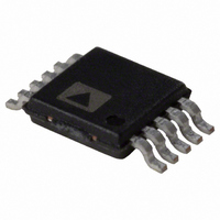
AD7686BRMZ Analog Devices Inc, AD7686BRMZ Datasheet - Page 6

AD7686BRMZ
Manufacturer Part Number
AD7686BRMZ
Description
IC ADC 16BIT 500KSPS 10-MSOP
Manufacturer
Analog Devices Inc
Series
PulSAR®r
Specifications of AD7686BRMZ
Data Interface
DSP, MICROWIRE™, QSPI™, Serial, SPI™
Number Of Bits
16
Sampling Rate (per Second)
500k
Number Of Converters
1
Power Dissipation (max)
21.5mW
Voltage Supply Source
Single Supply
Operating Temperature
-40°C ~ 85°C
Mounting Type
Surface Mount
Package / Case
10-TFSOP (0.118", 3.00mm Width)
Resolution (bits)
16bit
Input Channel Type
Pseudo Differential
Supply Voltage Range - Analogue
4.5V To 5.5V
Supply Voltage Range - Digital
1.8V To 5.8V, 2.3V To 5.8V
Sampling Rate
500kSPS
Rohs Compliant
Yes
Lead Free Status / RoHS Status
Lead free / RoHS Compliant
For Use With
EVAL-AD7686CBZ - BOARD EVALUATION FOR AD7686
Lead Free Status / RoHS Status
Lead free / RoHS Compliant, Lead free / RoHS Compliant
Available stocks
Company
Part Number
Manufacturer
Quantity
Price
Company:
Part Number:
AD7686BRMZ
Manufacturer:
ADI
Quantity:
1 000
Part Number:
AD7686BRMZ
Manufacturer:
ADI/亚德诺
Quantity:
20 000
Part Number:
AD7686BRMZ-REEL
Manufacturer:
ADI/亚德诺
Quantity:
20 000
Part Number:
AD7686BRMZ-RL7
Manufacturer:
ADI/亚德诺
Quantity:
20 000
Company:
Part Number:
AD7686BRMZRL7
Manufacturer:
ADI
Quantity:
1 000
Part Number:
AD7686BRMZRL7
Manufacturer:
ADI/亚德诺
Quantity:
20 000
AD7686
ABSOLUTE MAXIMUM RATINGS
Table 5.
Parameter
Analog Inputs
Supply Voltages
Storage Temperature Range
Junction Temperature
θ
θ
Lead Temperature Range
1
ESD CAUTION
ESD (electrostatic discharge) sensitive device. Electrostatic charges as high as 4000 V readily accumulate on
the human body and test equipment and can discharge without detection. Although this product features
proprietary ESD protection circuitry, permanent damage may occur on devices subjected to high energy
electrostatic discharges. Therefore, proper ESD precautions are recommended to avoid performance
degradation or loss of functionality.
See the
JA
JC
IN+
REF
VDD, VIO to GND
VDD to VIO
Digital Inputs to GND
Digital Outputs to GND
Thermal Impedance
Thermal Impedance
1
, IN−
Analog Input
1
section.
Rating
GND − 0.3 V to VDD + 0.3 V
or ±130 mA
GND − 0.3 V to VDD + 0.3 V
−0.3 V to +7 V
±7 V
−0.3 V to VIO + 0.3 V
−0.3 V to VIO + 0.3 V
−65°C to +150°C
150°C
200°C/W (MSOP-10)
44°C/W (MSOP-10)
JEDEC J-STD-20
30% VIO
1
2
2V IF VIO ABOVE 2.5V, VIO – 0.5V IF VIO BELOW 2.5V.
0.8V IF VIO ABOVE 2.5V, 0.5V IF VIO BELOW 2.5V.
t
DELAY
TO SDO
Figure 3. Load Circuit for Digital Interface Timing
2V OR VIO – 0.5V
0.8V OR 0.5V
Figure 4. Voltage Levels for Timing
50pF
C
L
Rev 0 | Page 6 of 28
500µA
500µA
2
1
I
I
OL
OH
Stresses above those listed under Absolute Maximum Ratings
may cause permanent damage to the device. This is a stress
rating only; functional operation of the device at these or any
other conditions above those indicated in the operational
section of this specification is not implied. Exposure to absolute
maximum rating conditions for extended periods may affect
device reliability.
70% VIO
t
DELAY
2V OR VIO – 0.5V
0.8V OR 0.5V
1.4V
2
1


