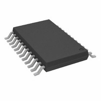
AD7730LBRU-REEL7 Analog Devices Inc, AD7730LBRU-REEL7 Datasheet - Page 21

AD7730LBRU-REEL7
Manufacturer Part Number
AD7730LBRU-REEL7
Description
IC ADC TRANSDUCER BRIDGE 24TSSOP
Manufacturer
Analog Devices Inc
Datasheet
1.AD7730LBRUZ.pdf
(52 pages)
Specifications of AD7730LBRU-REEL7
Rohs Status
RoHS non-compliant
Number Of Bits
24
Sampling Rate (per Second)
600
Data Interface
DSP, Serial, SPI™
Number Of Converters
1
Power Dissipation (max)
125mW
Voltage Supply Source
Analog and Digital
Operating Temperature
-40°C ~ 85°C
Mounting Type
Surface Mount
Package / Case
24-TSSOP (0.173", 4.40mm Width)
For Use With
EVAL-AD7730LEBZ - BOARD EVALUATION FOR AD7730EVAL-AD7730EBZ - BOARD EVAL FOR AD7730
REV. A
READING FROM AND WRITING TO THE ON-CHIP REGISTERS
The AD7730 contains a total of thirteen on-chip registers. These registers are all accessed over a three-wire interface. As a result,
addressing of registers is via a write operation to the topmost register on the part, the Communications Register. Figure 5 shows a
flowchart for reading from the different registers on the part summarizing the sequence and the words to be written to access each of
the registers. Figure 6 gives a flowchart for writing to the different registers on the part, again summarizing the sequence and words
to be written to the AD7730.
(SEE ACCOMPANYING TABLE)
COMMUNICATIONS REGISTER
WRITE BYTE W TO
READ REGISTER
CONTINUOUS
REQUIRED?
READS OF
REGISTER
START
COMMUNICATIONS REGISTER
(SEE ACCOMPANYING TABLE)
NO
WRITE TO REGISTER
WRITE BYTE Y TO
START
END
YES
Figure 5. Flowchart for Reading from the AD7730 Registers
(SEE ACCOMPANYING TABLE)
COMMUNICATIONS REGISTER
COMMUNICATIONS REGISTER
(SEE ACCOMPANYING TABLE)
NO
Figure 6. Flowchart for Writing to the AD7730 Registers
WRITE BYTE Y TO
WRITE BYTE Z TO
READ REGISTER
CONTINUOUS
OPERATION?
READ
STOP
YES
Register
Communications Register
Data Register
Mode Register
Filter Register
DAC Register
Offset Register
Gain Register
Test Register
–21–
Register
Status Register
Data Register
Mode Register
Filter Register
DAC Register
Offset Register
Gain Register
Test Register
*N/A= Not Applicable. Continuous reads of these registers does not make sense
as the register contents would remain the same since they are only changed by a
write operation.
Byte Y (Hex)
00
Read Only Register
02
03
04
05
06
User is advised not to change
contents of Test Register.
Byte W
10
11
12
(Hex)
13
14
15
16
17
AD7730/AD7730L
Byte Y
(Hex)
20
21
22
N/A*
N/A*
N/A*
N/A*
N/A*
Byte Z
(Hex)
30
30
30
N/A*
N/A*
N/A*
N/A*
N/A*


