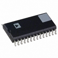
AD7708BRZ Analog Devices Inc, AD7708BRZ Datasheet - Page 30

AD7708BRZ
Manufacturer Part Number
AD7708BRZ
Description
IC ADC 16BIT R-R 8/10CH 28SOIC
Manufacturer
Analog Devices Inc
Datasheet
1.AD7708BRUZ-REEL.pdf
(44 pages)
Specifications of AD7708BRZ
Data Interface
DSP, MICROWIRE™, QSPI™, Serial, SPI™
Number Of Bits
16
Sampling Rate (per Second)
1.37k
Number Of Converters
1
Power Dissipation (max)
3.84mW
Voltage Supply Source
Analog and Digital
Operating Temperature
-40°C ~ 85°C
Mounting Type
Surface Mount
Package / Case
28-SOIC (0.300", 7.50mm Width)
Resolution (bits)
16bit
Input Channel Type
Pseudo Differential
Supply Voltage Range - Analogue
2.7V To 3.6V, 4.75V To 5.25V
Supply Voltage Range - Digital
2.7V To
Sampling Rate
105Hz
Rohs Compliant
Yes
Lead Free Status / RoHS Status
Lead free / RoHS Compliant
For Use With
EVAL-AD7708EBZ - BOARD EVAL FOR AD7708
Lead Free Status / RoHS Status
Lead free / RoHS Compliant, Lead free / RoHS Compliant
Available stocks
Company
Part Number
Manufacturer
Quantity
Price
Part Number:
AD7708BRZ
Manufacturer:
ADI/亚德诺
Quantity:
20 000
I/O Control Register (IOCON): (A3, A2, A1, A0 = 0, 1, 1, 1; Power-On-Reset = 00Hex)
The IOCON Register is an 8-bit register from which data can be read or to which data can be written. This register is used to con-
trol and configure the I/O port. Table XIX outlines the bit designations for this register. IOCON7 through IOCON0 indicate the
bit location, IOCON denoting the bits are in the I/O Control Register. IOCON7 denotes the first bit of the data stream. The num-
ber in brackets indicates the power-on/reset default status of that bit. A write to the IOCON register has immediate effect and does
not reset the ADCs.
Bit
Location
IOCON7
IOCON6
IOCON5
IOCON4
IOCON3
IOCON2
IOCON1
IOCON0
ADC Data Result Register (DATA): (A3, A2, A1, A0 = 0, 1, 0, 0; Power-On-Reset = 000000Hex)
The conversion result for the selected ADC channel is stored in the ADC data register (DATA). This register is 16 bits wide on the
AD7708 and 24 bits wide on the AD7718. This is a read only register. On completion of a read from this register the RDY bit in
the status register is cleared. These ADCs can be operated in either unipolar or bipolar mode of operation.
Unipolar Mode
In unipolar mode of operation the output coding is straight binary. With an analog input voltage of 0 V the output code is 0000Hex
for the AD7708 and 000000Hex for the AD7718. With an analog input voltage of 1.024 V
for the AD7708 and FFFFFF Hex for the AD7718. The output code for any analog input voltage can be represented as follows:
where
AIN is the analog input voltage and
N = 16 for the AD7708 and N = 24 for the AD7718.
AD7708/AD7718
I
O
C
(
) 0
O
N
7
I
Bit
Mnemonic
0
0
P2DIR
P1DIR
0
0
P2DAT
P1DAT
O
0
C
(
O
) 0
N
6
P
I
2
O
D
Table XIX. IOCON (I/O Control Register) Bit Designations
C
I
O
R
Description
This bit should always be cleared. Reserved for future use.
This bit should always be cleared. Reserved for future use.
P2, I/O Direction Control Bit.
Set by user to enable P2 as an output.
Cleared by user to enable P2 as an input. There are weak pull-ups internally when enabled
as an input.
P1, I/O Direction Control Bit.
Set by user to enable P1 as an output.
Cleared by user to enable P1 as an input. There are weak pull-ups internally when enabled
as an input.
This bit should always be cleared. Reserved for future use.
This bit should always be cleared. Reserved for future use.
Digital I/O Port (P1) Data Bit.
The readback value of this bit indicates the status of the pin regardless of whether this pin is
configured as an input or an output. The value written to this data bit will appear at the
output port when the I/O pin is enabled as an output.
Digital I/O port (P1) Data Bit.
The readback value of this bit indicates the status of the pin, regardless of whether this pin is
configured as an input or an output. The value written to this data bit will appear at the
output port when the I/O pin is enabled as an output.
N
(
) 0
5
Code = (AIN × GAIN × 2
P
I
O
1
D
C
I
O
R
N
(
) 0
4
I
O
0
C
(
O
) 0
N
N
)/(1.024 × V
3
I
O
0
C
(
REF
O
) 0
N
)
2
REF
P
/Gain the output code is FFFFHex
I
2
O
D
C
A
O
T
N
(
1
) 0
P
I
1
O
D
C
A
O
T
N
(
0
) 0


